
Solder Joint Failure: WHITE PAPER
SERIES Part 1: The Journey of an Electronic Device Through the Analytical Lab
In the first article of this series, you will experience the steps of a typical workflow used to analyze solder joint failure and characterize a suspect solder joint. Future articles will explore specific processes in greater detail.
Table of Contents
| 1 | Finding the Problem |
| 2 | Non-destructive Testing |
| 3 | Sample Preparation |
| Sectioning | |
| Mounting | |
| Grinding & Polishing | |
| 4 | Image Analysis |
| Optical Image Analysis | |
| SEM Image Analysis | |
| 5 | Conclusion |

1 Finding the Problem
Today there are many technologies available to help us understand issues with assembled electronics. In part one of this series of articles we take you on a tour of a faulty electronic device through the analytical lab.
You will gain knowledge of the steps required to understand electronic device failure. Read on to discover what you can do to better understand the problem and characterization of solder joints.
Future articles in this series will focus on the specific capabilities required and details of the processes described here.
We received a circuit board in the analytical lab with the indication that the board was not functioning properly. We electrically tested the PCB and diagnosed the fault at the ball grid array (BGA)
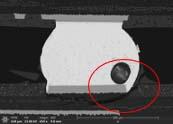
Our initial approach was to use 2D X-ray to take a closer look at the solder bumps.
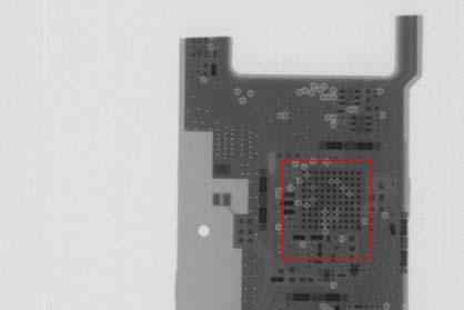
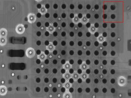
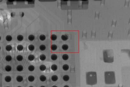
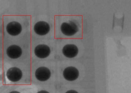
At low magnification and low power, we did not find a potential fault with the exception of the solder bump in the upper right corner. The solder joint density does not seem to be normal, possibly indicating missing solder or a lifted solder pad.
Using 2D X-ray we increase the power and tilt the detector to get a much better view of the solder joint. In doing so we see the problem. It appears some damage has occurred, in addition to some voiding in a number of the other solder bumps.
We could do a void analysis here, however we really want to understand the bigger issue of damage to the solder bump in the upper right-hand corner.
2 Non-destructive Testing
One option here would be to rework and replace the BGA, then electrically test and consider the work complete. However, the customer has additional concerns that require further analysis.
Thus far, we have performed non-destructive testing and analysis. This implies that we would be able to repair the device. The additional solder joint failure analysis required uses destructive testing methods, which will render the device unusable.
3 Sample Preparation
Properly preparing the sample for additional analysis is critical to get the best results possible. A skilled, experienced technician with a background material science, metallurgy and physics will complete the process accurately and in a reasonable timeframe.
Many new start-up labs use a lab service company, such as JH Analytical, to help define the process prior to bringing it in-house. This saves significant time and cost in addition to:
- Enabling full use of lab equipment that might not otherwise be available
- Helping you develop an understanding of the requirements for an internal lab
- Highly trained experts that understand the techniques perform the work and help you develop your process
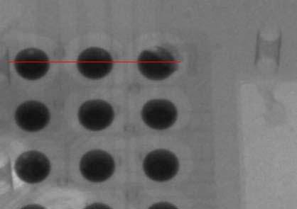
Sectioning the Failed Solder Joint
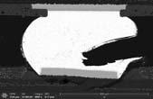
Initial destructive testing begins with sample preparation in the wet lab. The first step is to cut the BGA precisely where the solder joint problem is most pronounced. The red line indicates the primary cutting plane.
We used a Buehler Isomet High Speed Sectioning Saw to precisely cut the sample into a small enough size to allow mounting.
The Isomet is designed to precisely cut samples of any material makeup.

Mounting
Mounting is the process of embedding the cut sample into an epoxy puck. This makes the sample easier to handle and enables the use of automated tools. The sample can then be ground and polished with the precision needed to perform image analysis.
It is critical that the epoxy system used is void free, in particular with softer materials such as plastics.
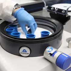
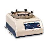
Void free encapsulation prevents smearing during the grinding and polishing process and creates the highly defined smudge free surface needed for proper image analysis. Pictured here is the Buehler Simplivac Cold Mount Vacuum System used to remove air from epoxy cups to create better adhesion to the sample.
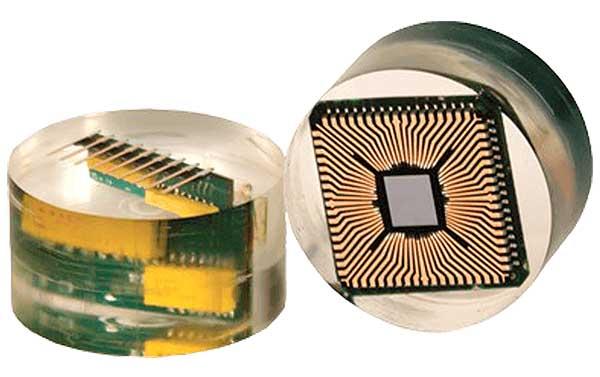
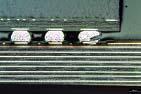
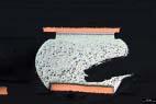
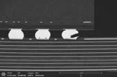
Below are typical samples of epoxy mountings after curing. Typical epoxy puck size is 1.25”, and they can be as large as 2.0”.
Grinding and Polishing
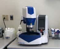
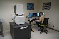
The next step in the sample preparation process is grinding and polishing. This is a critical step prior to imaging and generally requires an experienced technician to garner the best results. Imaging quality is 100% dependent on the quality of the grinding and polishing process. Our lab features two Buehler grinders and polishers with automated capability. Combined with our lab manager’s 20+ years of experience these tools help us get the best result possible.
4 Solder Joint Failure Image Analysis
Optical Image Analysis
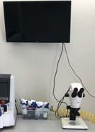
Upon completion of the polishing process, we are ready for imaging and microscopic analysis. The newest Leica optical and digital microscopes enable detailed image analysis including measurement, particle analysis, grain sizing and more.

Below are typical images of a properly prepared sample for optical image analysis.
SEM Image Analysis
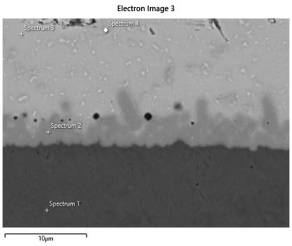
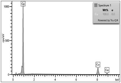
In addition to highly detailed images, we sometimes require additional information to fully characterize the failure. To accomplish this, we use a Thermofisher Apreo S field emission scanning electron microscope (SEM), which offers the latest in SEM technology.
Matched with an EDS (energy-dispersive x-ray spectroscopy) system from Oxford Instruments, we can fully characterize the problem and completely understand the material makeup of the failed solder joint.
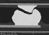
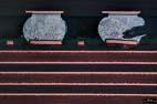
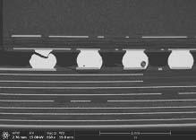
Images, L to R: Solder Crack Magnified, Older Voiding and PCB Crack, Magnified, Damaged Solder ball, Close-up of Solder Ball Damage
Additional high magnification images reveal microcracking in the intermetallic layer of the damaged areas.
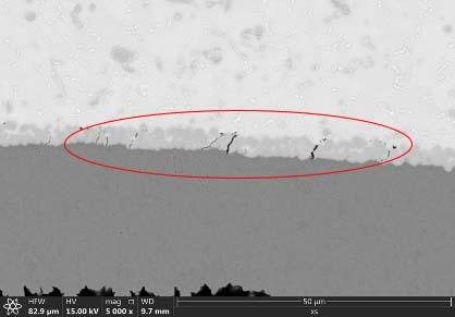
Micro Cracks in Solder
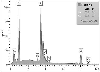
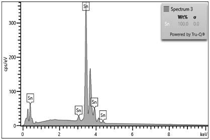
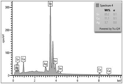
A material structure analysis reveals all of the elements present in the damaged areas. These elements include carbon, tin, copper, silver, barium and nickel.
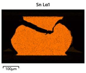
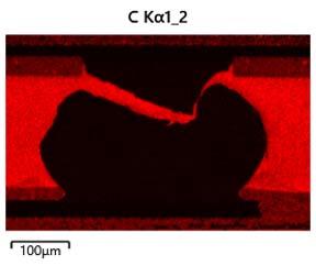
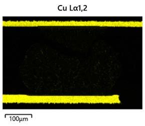
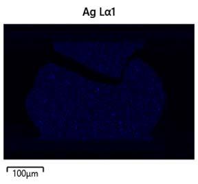
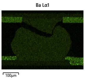
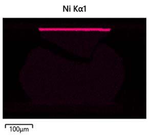
The SEM is able to capture quantitative data about the makeup of this solder joint and the intermetallic layer created during soldering.
5 Conclusion
You have seen how a solder joint failure problem travels through the analytical lab. We have just skimmed the surface. Stay tuned as we develop each section above in greater detail.
Please complete the form above or contact JH Analytical for additional information or assistance with your application.
Get Application Support
KNOW WHAT YOU'RE LOOKING FOR?
QUICKLY SEARCH THOUSANDS OF PRODUCTS...

Recent Posts


