Cone Beam CT vs. Oblique CT: Choosing the Right X-Ray Inspection Technique for 3D Analysis
Recent Blogs Cone Beam CT vs. Oblique CT: Choosing the
Compact vs. High-End EBSD Systems: A Performance Comparison of Detector Technologies
Recent Blogs Compact vs. High-End EBSD Systems: A Performance Comparison

SEM: Low Vaccuum vs. High Vacuum Imaging – Webinar
Recent Blogs 5 Key Takeaways from Our Webinar: Low Vacuum

What Happens When Elves Discover Surface Metrology?
Recent Blogs What Happens When Elves Discover Surface Metrology? Candy

2025 Equipment Tax Benefits to Consider
Recent Blogs Equipment Tax Benefits for 2025! Is Now the
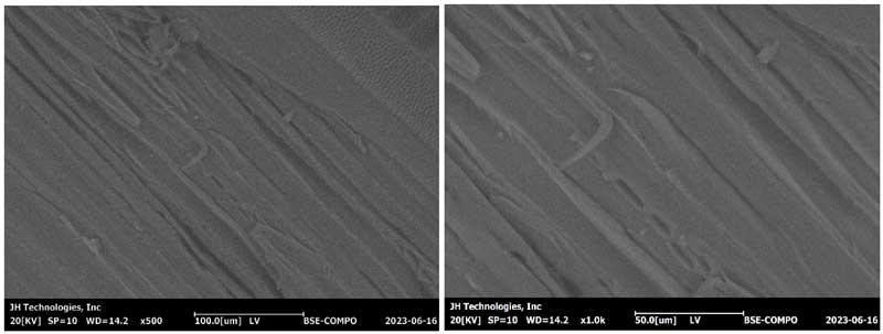
However, when imaged under low-vacuum conditions, the pine wood sample exhibits no charge accumulation, resulting in improved contrast and finer details, thanks to the application of a higher energy 20kV beam and reduced charge accumulation.
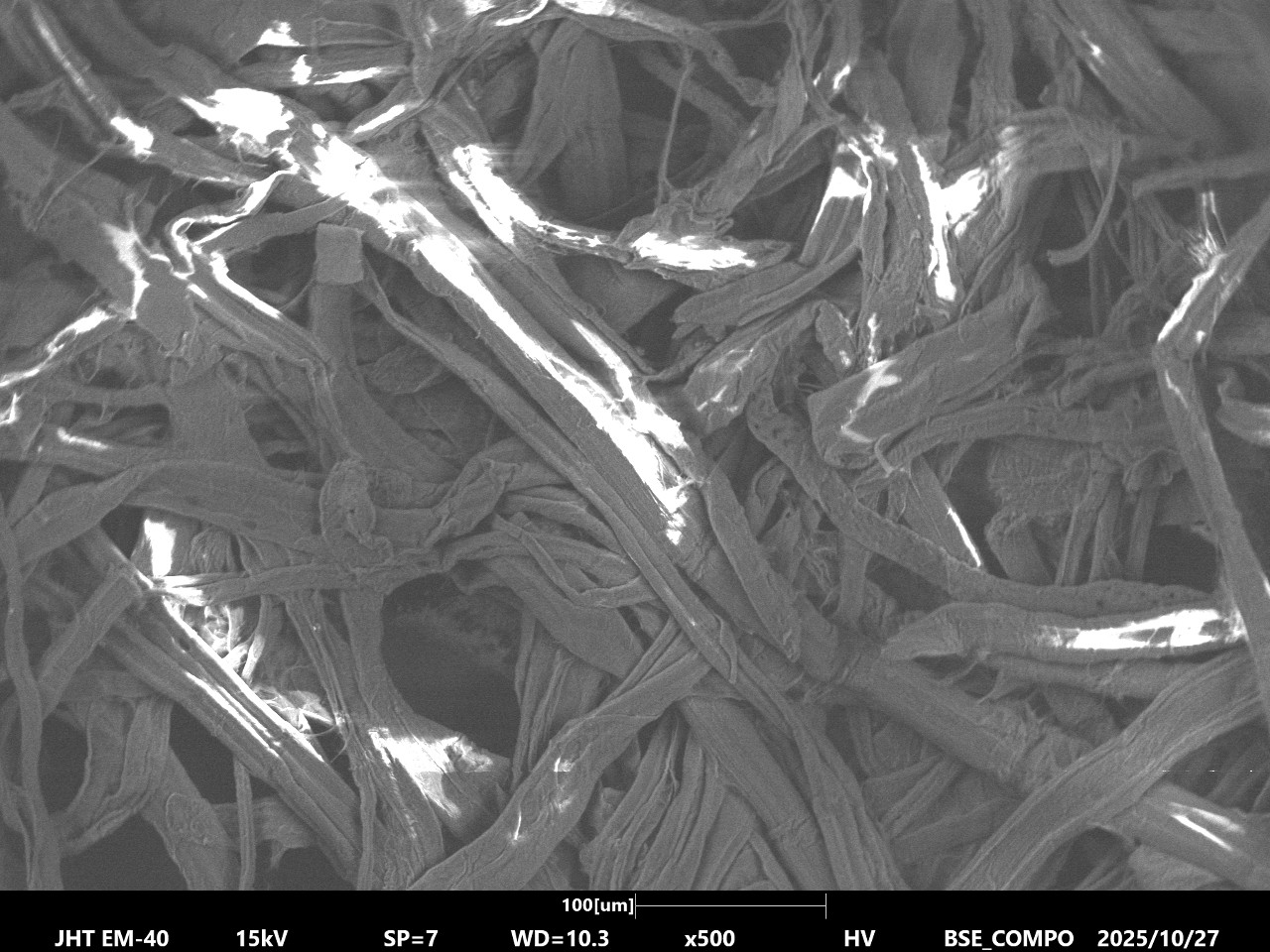
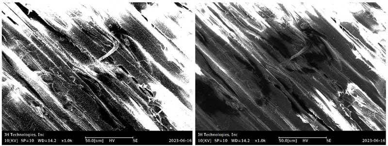
Here is an example of a paper towel imagied with High Vacuum, and no coating
Here is the same example imaged High Vacuum, and coated with a thin layer (5nm) of gold

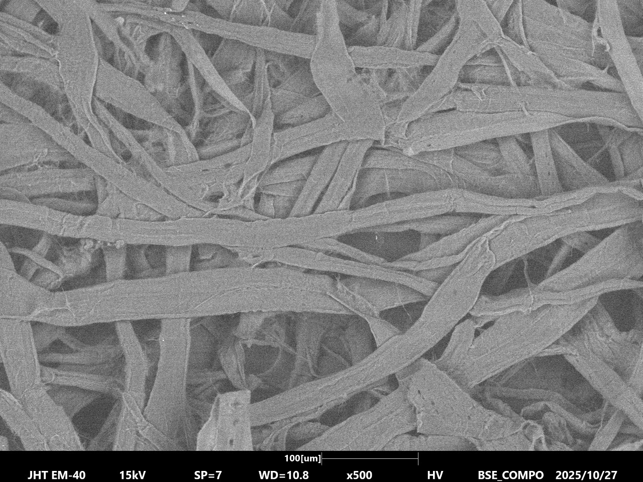
Here is the same sample imaged at Low Vacuum showing a more detailed clearer image.