What Happens When Elves Discover Surface Metrology?
Recent Blogs What Happens When Elves Discover Surface Metrology? Candy

2025 Equipment Tax Benefits to Consider
Recent Blogs Equipment Tax Benefits for 2025! Is Now the
Reviving Legacy AFMs: How to Unlock New Capabilities
Recent Blogs Reviving Legacy AFMs: How to Unlock New Capabilities

Automotive Paint Layer Analysis with Microscopy & EDS | JH Technologies
Recent Blogs Automotive Paint Layer Analysis with Optical Microscopy, SEM,
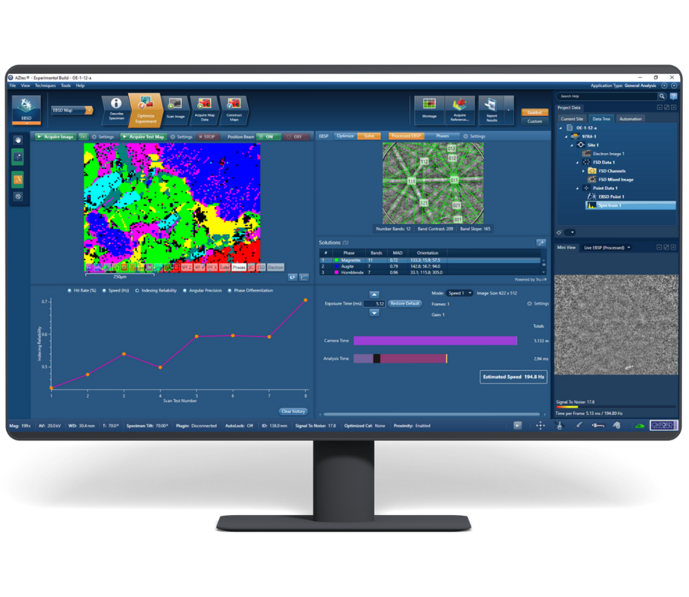
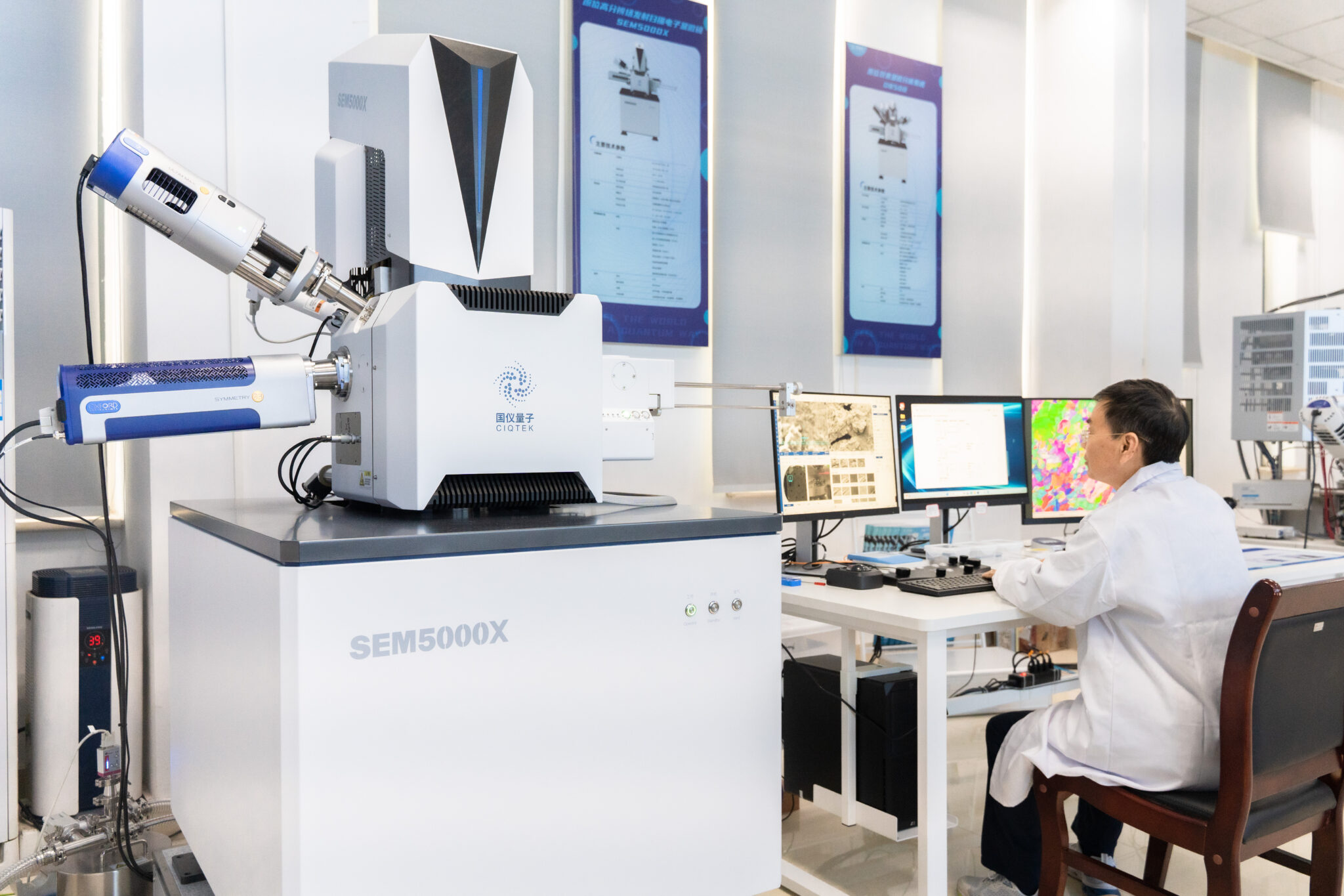
What Is EBSD? A Guide to Electron Backscatter Diffraction in SEM
Recent Blogs A Guide to Electron Backscatter Diffraction (EBSD) Electron

– **Tabletop SEMs** (e.g., Coxem EM-40 with Bruker e-Flash XS): Cost accessible and compact, suitable for basic orientation and phase mapping on coarse-grained or high-contrast systems. Indexing speeds from 50 – 200 points/second.
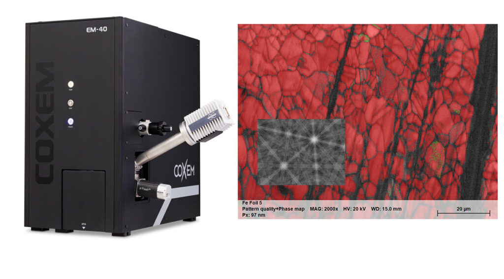 Coxem EM-40 with compacts EDSB – Photo courtesy of Coxem
2. EBSD Detector and Optics
High-sensitivity EBSD detectors (CMOS or sCMOS-based) with optimized phosphor screens and fiber optics are required to resolve clear Kikuchi patterns. Detector placement, solid angle, and lens configuration impact pattern clarity and acquisition rates.
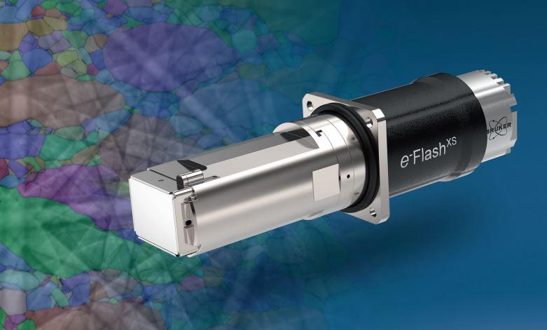 Compact EBSD detector for table-top SEM – Photo courtesy of Bruker