Header logo
Contact

Memory Device Cross-Sectioning [Learn from the JHA Team]

magnified DRAM lead

Producing Memory Device Cross-Sectiong Samples

Our newest JH Analytical Team member David is supporting and learning all of the functions in the lab.

What better way to learn than to produce some cross-section samples on your own!

We gave David a DRAM memory card and asked him to create cross-section samples to help our sales staff show Leica optics capabilities.

Below is a step-by-step pictorial view of our memory device cross-sectioning sample preparation process and final results.

A Day in the Analytical Lab

David and our intern Alex Lau created these samples in roughly one day while learning the ins-and-outs of processing electronic devices for analysis.

The samples came out great and you can see the resulting images below.

Different Imaging Methods Offer Different Results

We used different imaging methods to show the results you can expect. Each method has benefits, in addition to providing information and data.

The best method for memory device cross-sectioning and other analytical lab processes is the one that provides the data you need in the most cost-effective way.

As both a supplier and user of the tools used to generate the images below, we have the unique advantage of choosing the most appropriate tool for the job.


We invite you to visit our lab and see all that can be done to get you the answers you need. Complete the form on this page or give us a call at 408-436-6336 for assistance.


Memory Device Cross-Sectioning Process and Imaging Equipment

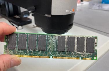
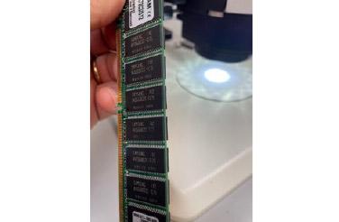
1. Entire DRAM Memory Board

DRAM Memory Board

1a) DRAM Memory Macro View

DRAM Memory Macro View

Image taken on Leica DVM6 M optical microscope.
Here you can see the device prior to sectioning.

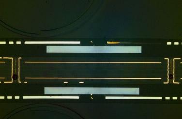
1b) DRAM Memory Single Lead Macro View

DRAM Memory SIngle Lead Macro View

 Magnified to see lead #1 prior to sectioning.
Image taken on Leica DVM6 M.

2) DRAM Memory Board After Initial Sectioning

DRAM Memory Board, sectioned

Device has been cut deep enough into the package to see the first two leads and the chip inside.

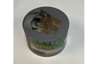
2a) Completed Section of DRAM Memory Sample After Mounting and Polishing

Polished DRAM Module

Sample mounted on Buehler Simplivac and polished on Buehler Automet 250.

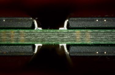
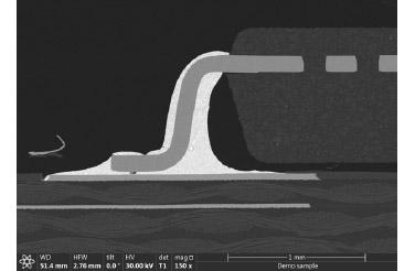
3) DRAM Memory Low Mag Cross-Section

DRAM Memory Low Mag Cross-Section

Image taken on Thermofisher Apreo S FSEM.

3a) DRAM Memory High Mag

DRAM Memory High Mag

Image taken on Leica DVM6 M.

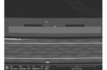
3b) DRAM Memory Low Mag

DRAM Memory Low Mag

Image taken on Thermofisher Apreo S FSEM.

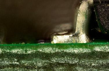
4) DRAM Memory Single Lead High Mag

DRAM Memory Single Lead Hi-Mag

Image taken on Leica DM2700 M in DIC.

4a) DRAM Memory Single Lead Low Mag

DRAM Memory Single Lead Lo-Mag

Image taken on SEM.

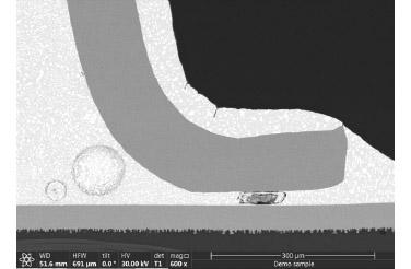
4b) DRAM Memory Single Lead High Mag Showing Grain Structure

DRAM Memory Single Lead Grain Structure

Image taken on Thermofisher Apreo S FSEM.

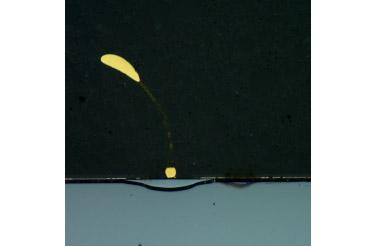
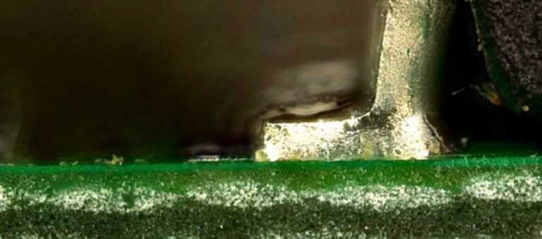
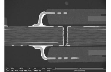
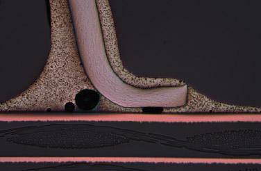
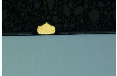
5) DRAM Memory Wire Bond Low Mag

DRAM Memory Wire Bond Low Mag

Image taken on Leica DVM6 M-Brightfield Illumination.

5a) DRAM Memory Wire Bond High Mag Darkfield Illumination

DRAM Memory Wire Bond High Mag Darkfield

Image taken on Leica DVM6 M-Darkfield Illumination.

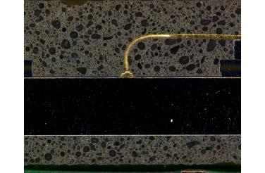
5b) DRAM Memory Wire Bond High Mag

DRAM Memory Wire Bond High Mag

Image taken on DVM6 M-Brightfield Illumination.

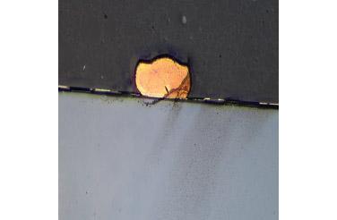
5c) DRAM Memory Wire Bond High Mag EDF (Extended Depth of Field)

DRAM Memory Wire Bond High Mag Extended Depth of Field

Image taken on Leica DVM6 M.

Get Application Help

Yes
No

Recent Articles