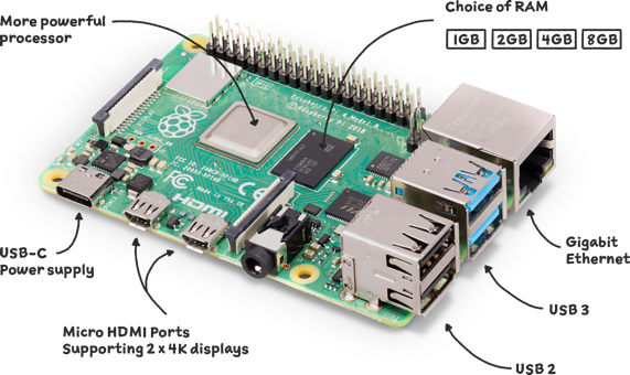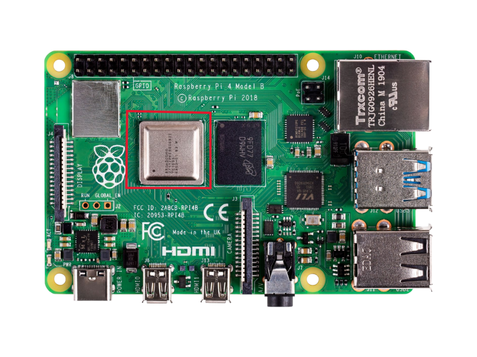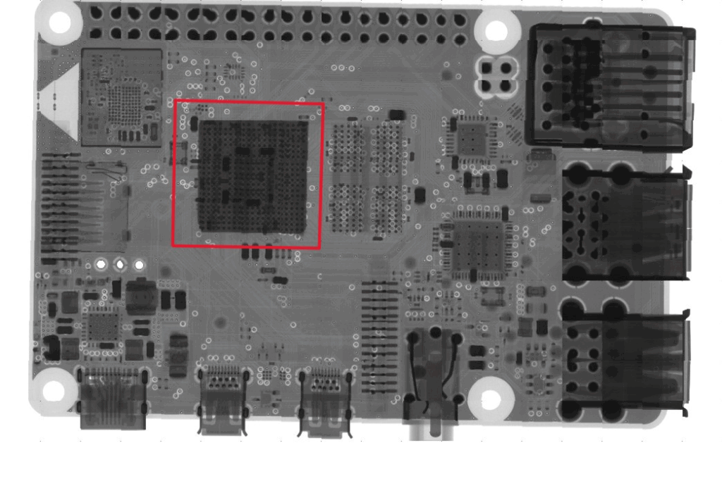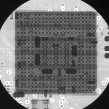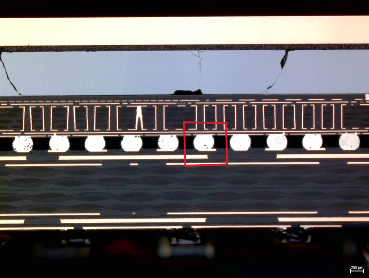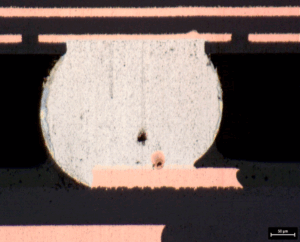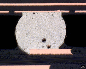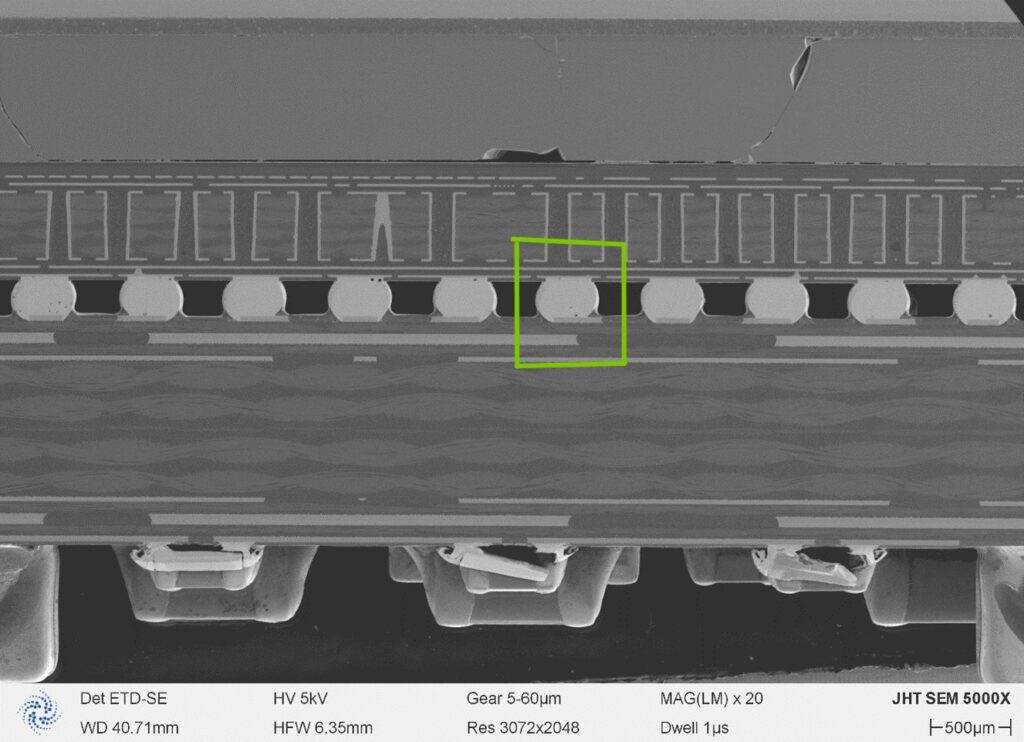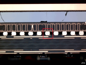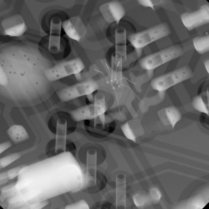
Cone Beam CT vs. Oblique CT: Choosing the Right X-Ray Inspection Technique for 3D Analysis
Recent Blogs Cone Beam CT vs. Oblique CT: Choosing the
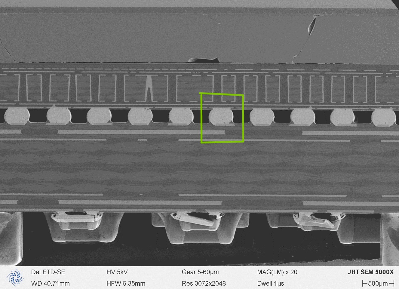
Compact vs. High-End EBSD Systems: A Performance Comparison of Detector Technologies
Recent Blogs Compact vs. High-End EBSD Systems: A Performance Comparison

SEM: Low Vaccuum vs. High Vacuum Imaging – Webinar
Recent Blogs 5 Key Takeaways from Our Webinar: Low Vacuum

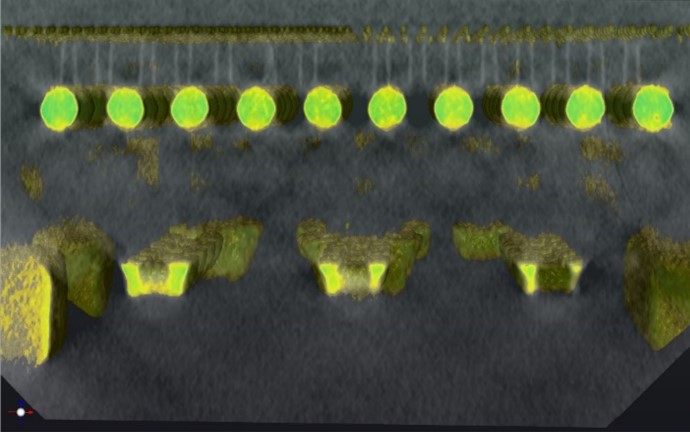
What Happens When Elves Discover Surface Metrology?
Recent Blogs What Happens When Elves Discover Surface Metrology? Candy

2025 Equipment Tax Benefits to Consider
Recent Blogs Equipment Tax Benefits for 2025! Is Now the