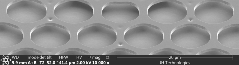
Memory Device Cross-Sectioning [Learn from the JHA Team]
Recent Blogs Memory Device Cross-Sectioning [Learn from the JHA Team]...
Read More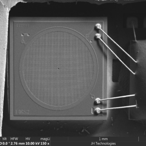
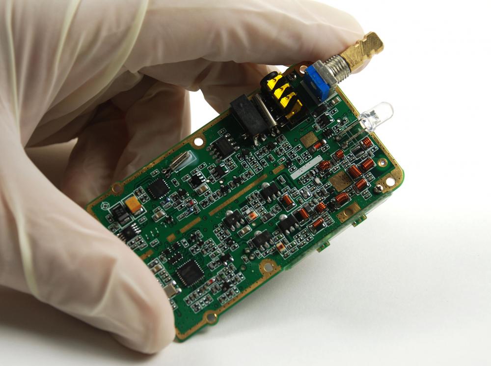
Solutions for Semiconductor Applications
Recent Blogs Solutions for Semiconductor Applications JH Technologies is pleased...
Read More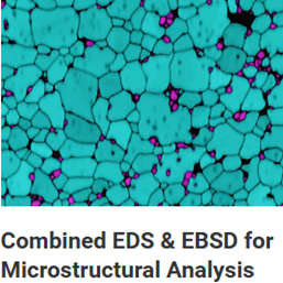
Bruker EDS & EBSD
Recent Blogs EDS & EBSD for SEM Adding Bruker EDS to your...
Read More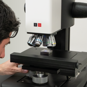
New S lynx 2 Optical Surface Profiler
Recent Blogs New S lynx 2 Optical Surface Profiler A...
Read More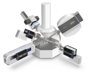
SEM Detectors – EDS, EBSD, and Micro-XRF
Our portfolio covers tabletop and floor-model SEMs from Oxford Instruments...
Read More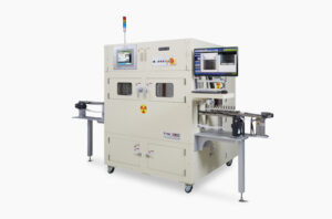
Industrial X-Ray Inspection Systems | NDT Equipment
Explore high-performance x-ray inspection systems for electronics, batteries, semiconductors, and...
Read More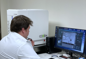
SEM’s: Tabletop & Compact Floor Standing
Unlock the full potential of high-performance tabletop SEM capabilities with...
Read More
High Resolution Scanning Electron Microscopes—Full Size
Unlock the full potential of high-performance tabletop SEM capabilities with...
Read More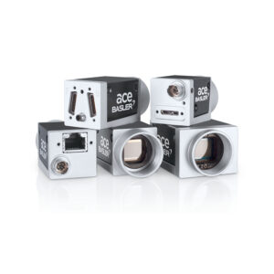
Accessories and Lenses
Complementing our comprehensive instrument offerings, we provide a diverse range...
Read More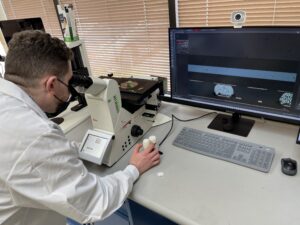
JH Analytical Services
Our analytical laboratory provides specialized testing and characterization services across...
Read More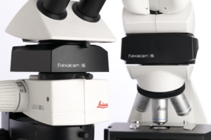
Microscope Cameras And Software
In the rapidly evolving world of microscopy, having the right...
Read More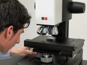
Metrology and 3D Surface Profiling
In the realms of scientific research, industrial inspection, and quality...
Read More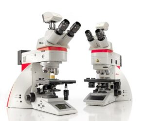
Compound Upright Microscopes
Compound microscopes for applications including education, materials manufacturing and research,...
Read More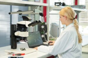
Ergonomic Routine Stereo Microscopes
The standard in ergonomic microscopy. For users doing repeated rework...
Read More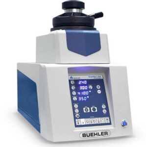
Metallography Sample Preparation Equipment
We understand the complexities involved in materials preparation and analysis....
Read More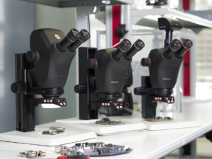
Routine Inspection/Assembly Microscopes
Maximize quality control and achieve flawless assembly with our durable,...
Read More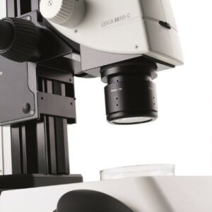
Ergonomic Research Stereo Microscopes
Reproducible results are crucial in imaging, especially when capturing intricate...
Read More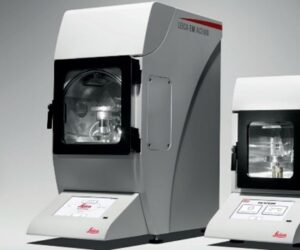
Electron Microscopy Sample Preparation
Preparing samples flawlessly is crucial for obtaining top-notch electron microscope...
Read More
Digital Microscope
In the era of cutting-edge technology, digital microscopes have revolutionized...
Read More