Recent Blogs

What Happens When Elves Discover Surface Metrology?
Recent Blogs What Happens When Elves Discover Surface Metrology? Candy

2025 Equipment Tax Benefits to Consider
Recent Blogs Equipment Tax Benefits for 2025! Is Now the

Reviving Legacy AFMs: How to Unlock New Capabilities
Recent Blogs Reviving Legacy AFMs: How to Unlock New Capabilities

Automotive Paint Layer Analysis with Microscopy & EDS | JH Technologies
Recent Blogs Automotive Paint Layer Analysis with Optical Microscopy, SEM,

What Is EBSD? A Guide to Electron Backscatter Diffraction in SEM
Recent Blogs A Guide to Electron Backscatter Diffraction (EBSD) Electron
What Is Ion Milling? A Guide to SEM Sample Preparation Using Ion Beam Technology
What is Ion Milling?
Ion milling is a precision sample preparation technique that uses a high-energy ion beam to remove surface material from a sample. It is especially useful for preparing samples for scanning electron microscopy (SEM) and analytical techniques such as EDS (energy-dispersive X-ray spectroscopy) and EBSD (electron backscatter diffraction).
This non-contact method helps reveal fine surface structures, eliminate mechanical polishing damage, and prepare smooth, artifact-free surfaces.
Ion Milling vs. Focused Ion Beam (FIB)
There are two common types of ion beam milling systems:
- Broad Beam Ion Milling: Uses a wide-area ion beam to uniformly etch large surface areas. Ideal for SEM prep and flat milling.
- Focused Ion Beam (FIB) Milling: Uses a tightly focused beam to selectively mill very small regions. Common in failure analysis and TEM prep.
At JH Technologies, we primarily use broad beam ion milling systems to prepare cross-sections and surface finishes for high-resolution imaging.
What Types of Samples Can be Ion Milled?
Ion milling is versatile and works across a broad range of materials, including:
- Electronics and semiconductors
- Metals and alloys
- Ceramics and composites
- Polymers and soft materials
- MEMS and multilayer devices
Key Benefits of Ion Milling for Sample Preparation
Ion milling offers several advantages over mechanical polishing and chemical etching:
- Non-contact process: Avoids scratching, smearing, and deformation
- Ideal for soft and delicate materials: Especially important for polymers and heat-sensitive samples
- Improved EBSD performance: Produces flat, damage-free surfaces for better indexing
- Cryogenic compatibility: Optional cooling stages prevent thermal damage
- Excellent for composite samples: Polishes soft and hard materials side-by-side without smearing
Whether you’re preparing a solder joint, a polymer interface, or a cross-section of a MEMS device, ion milling helps preserve structural integrity and enhance imaging results.
Related Ion Milling in SEM Sample Preparation Content
Ion milling supports a wide range of advanced imaging and analysis applications. Below are real-world examples showing how researchers and engineers use ion milling to prepare high-quality samples for SEM, EDS, EBSD, and more.
Lithium Battery Sample Preparation
Learn how ion milling is used to expose internal structures in lithium-ion batteries for failure analysis and quality control.
Micro Cracks in Solder Joints
Ion milling reveals fine microcracks in solder joints, enabling more accurate failure detection in electronic assemblies.
Analyzing a MEMS Microphone
Explore how ion milling enables precise cross-sectioning of MEMS devices—critical for evaluating layered structures and internal interfaces.
EBSD Sample Preparation Best Practices
Discover how ion milling improves EBSD results by creating flat, damage-free surfaces that enhance pattern quality and indexing accuracy.
Polishing Soft Materials
Ion milling is ideal for polishing polymers, composites, and soft materials that would otherwise deform or smear under mechanical prep.
Learn More About JH Technologies’ Ion Milling Solutions
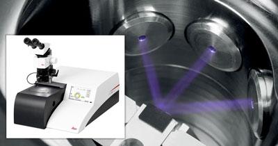
JH Technologies offers a full range of ion milling equipment from Coxem and Leica, including broad beam systems and accessories like cryo stages and vacuum transfer docks.
Explore our wide range of ion milling equipment and request a quote today!


