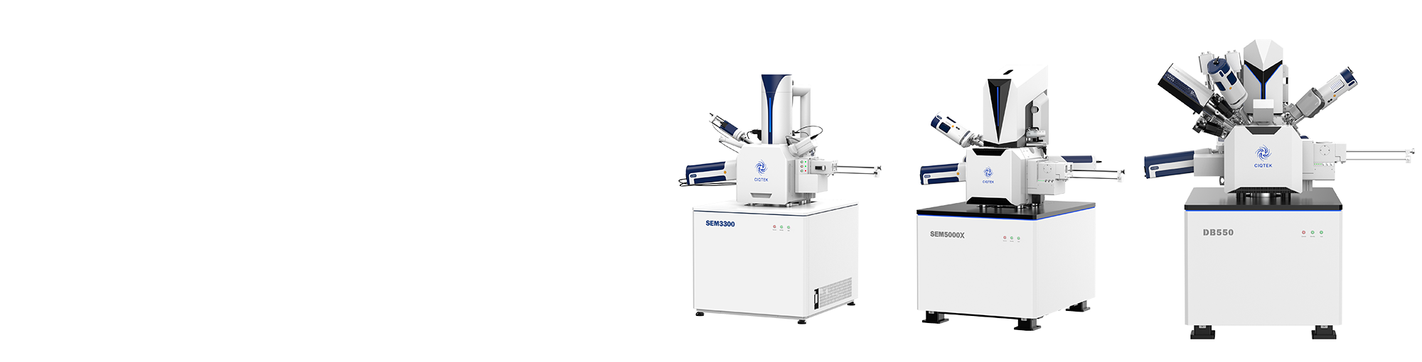
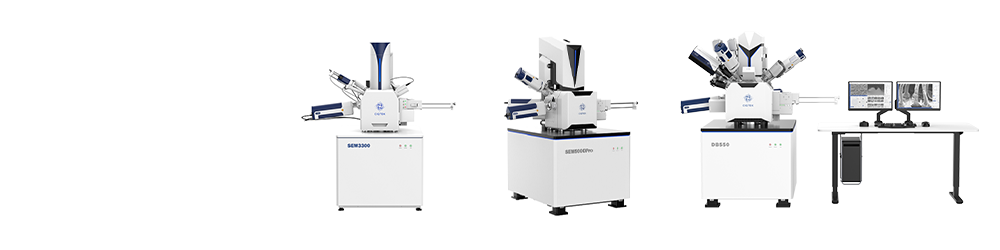
High Resolution Scanning Electron Microscopes—Full Size
JH Technologies offers a range of high-resolution scanning electron microscopes (SEMs) from CIQTEK, combining advanced imaging, user-friendly software, and affordability. Designed for materials science, semiconductor research, and failure analysis, these systems deliver the precision and reliability needed to drive innovation and maintain efficient workflows.
Selecting the right scanning electron microscope (SEM) depends on your imaging needs, sample type, resolution requirements, and workflow priorities. JH Technologies’ high resolution SEM systems are each tailored to specific research and industrial applications.
Whether you’re focused on surface topography, compositional analysis, or microstructural characterization, JH Technologies has a solution engineered to meet your needs. Explore the models below or contact us to discuss your application.
Tungsten Filament SEM–Affordable, Advanced Electron Microscopy
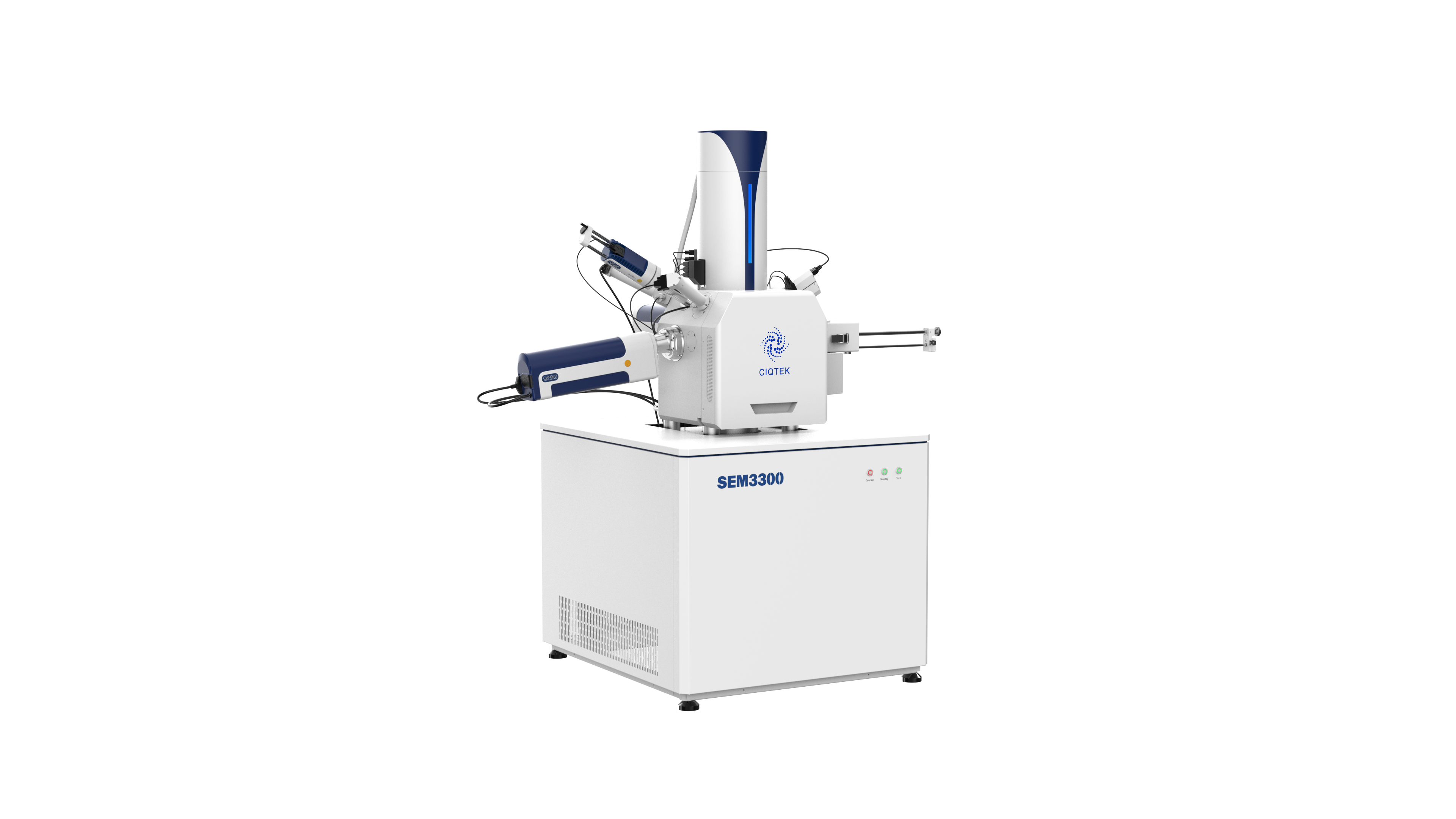
Engineered for routine imaging and inspection, materials characterization and quality control, a tungsten scanning electron microscope offers excellent versatility and ease of use. The CIQTEK Tungsten Filament SEM provides reliable high-resolution imaging and elemental analysis at an affordable price in fields such as materials science, electronics, and manufacturing.
Full-Size Field Emission SEM (FE-SEM)–Ultra-High Resolution Imaging
Field emission scanning electron microscopes (FE-SEMs) offer enhanced resolution and surface detail for high-precision imaging at nanoscale. The CIQTEK Full-Size Field Emission SEM delivers ultra-high-resolution performance for advanced applications in semiconductors, materials science, and nanotechnology.
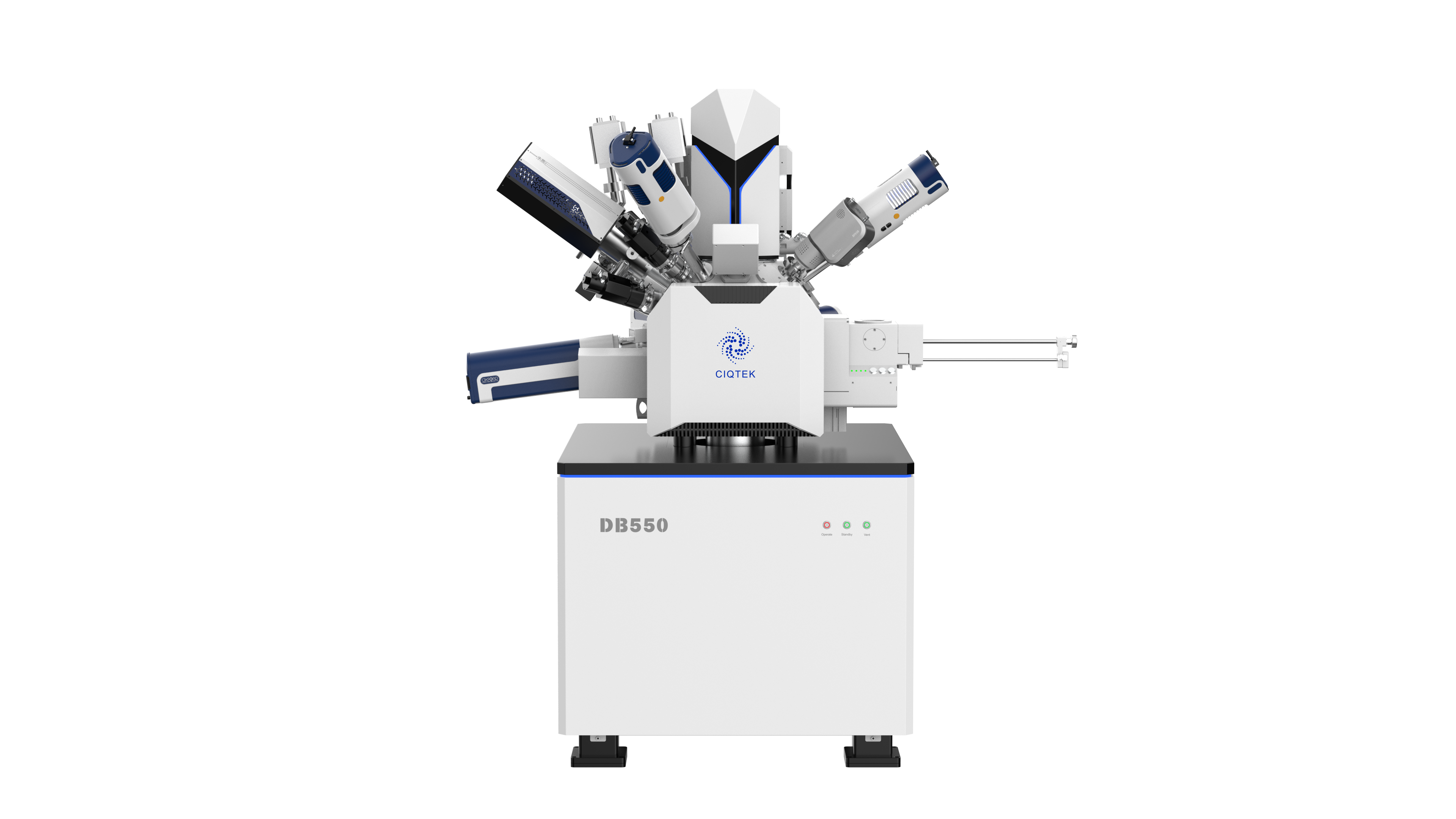
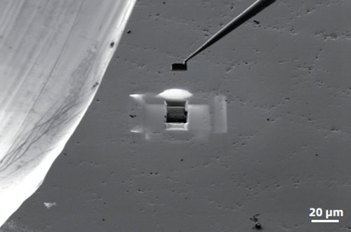
Focused Ion Beam SEM (FIB-SEM)–Integrated Ion Milling
Focused Ion Beam scanning electron microscopes (FIB-SEMs) combine ion beam milling with high-resolution imaging for advanced analysis, fabrication, and sample preparation. The CIQTEK FIB-SEM delivers precise nanoscale modification and imaging in one integrated system—ideal for failure analysis, cross-sectioning, and 3D tomography.
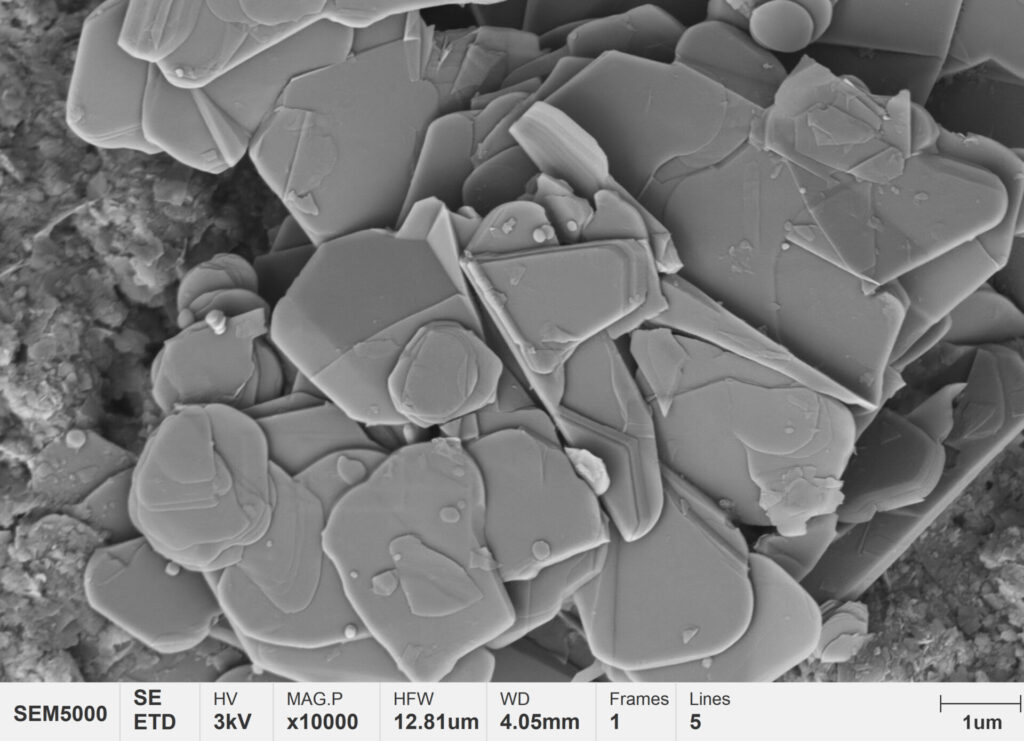
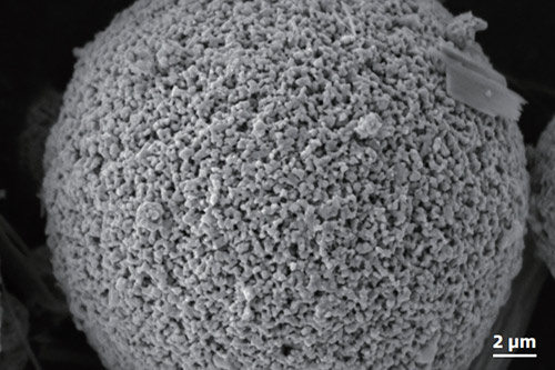
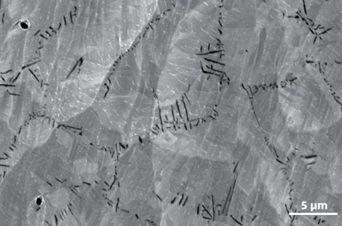
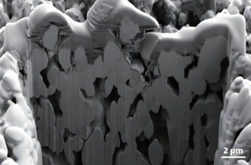
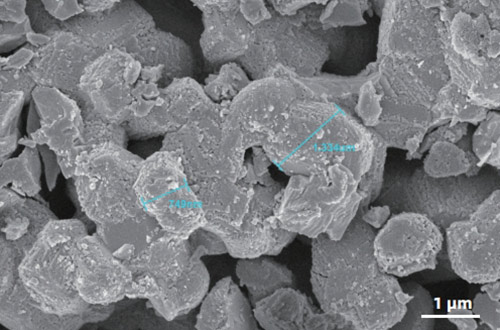
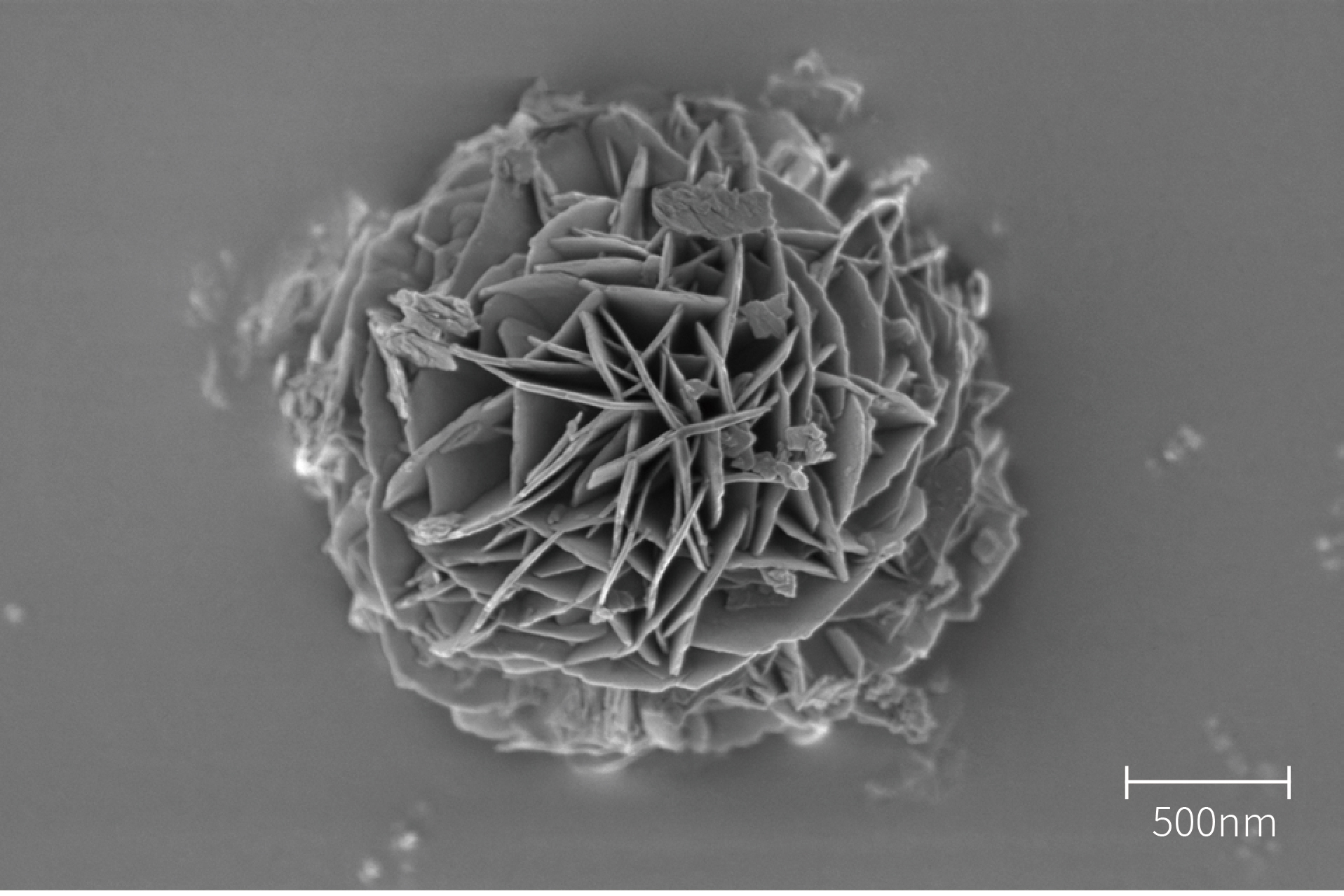
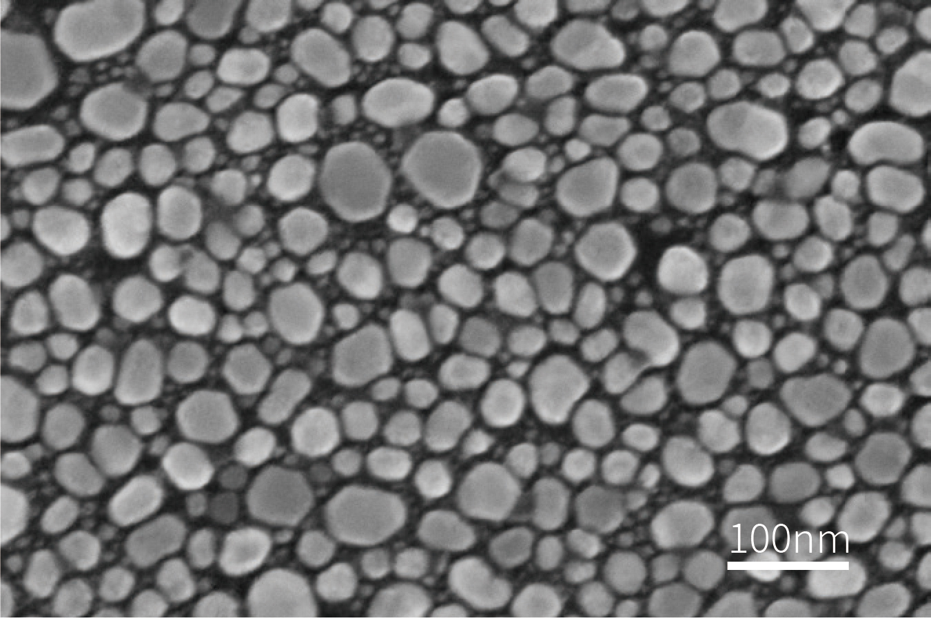
CIQTEK’s scanning electron microscopes are built to deliver detailed, high-resolution imaging across a wide range of sample types and materials. Whether you’re analyzing metals, ceramics, or battery materials, CIQTEK SEMs provide the clarity and contrast researchers and engineers rely on for accurate surface and structural characterization.
Above are a few real-world imaging examples captured using CIQTEK SEM systems.
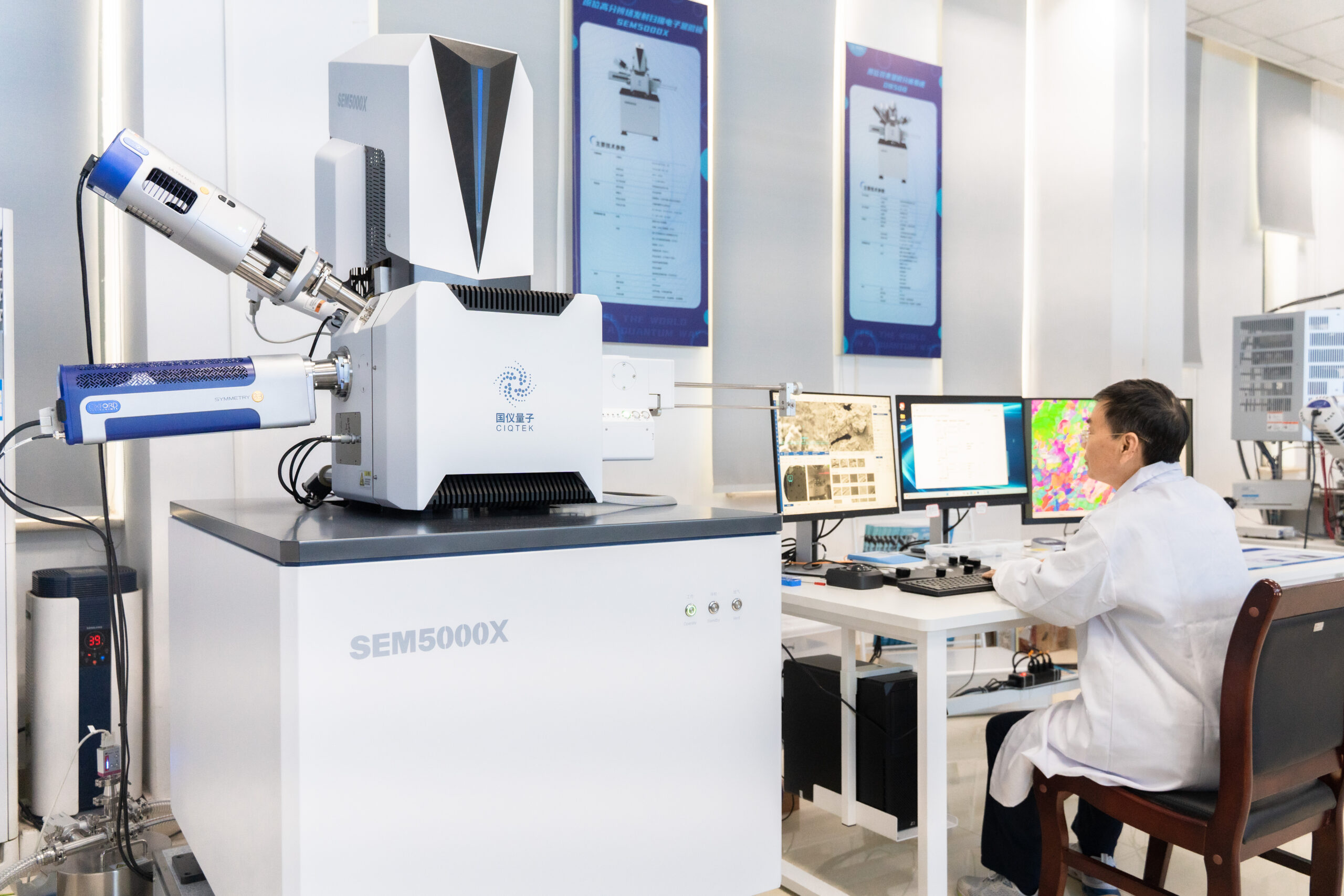
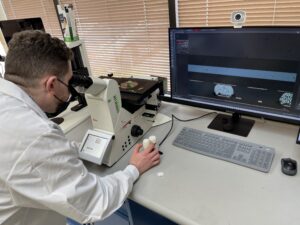
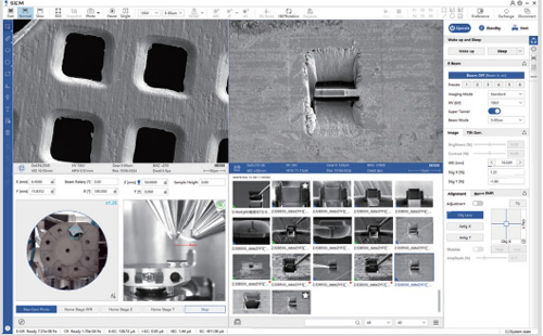
CIQTEK’s scanning electron microscope software is engineered to simplify complex workflows without compromising control. With an intuitive interface and integrated imaging and processing tools, users can navigate system functions, view live comparative data, and control advanced accessories—all from a single platform.
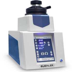
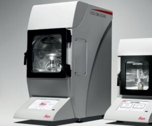
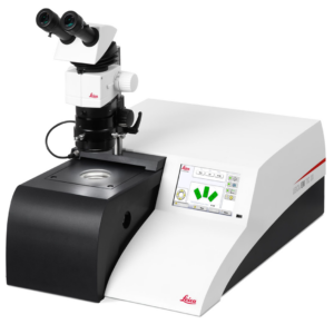
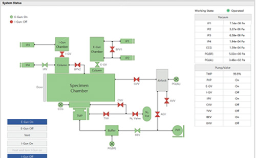
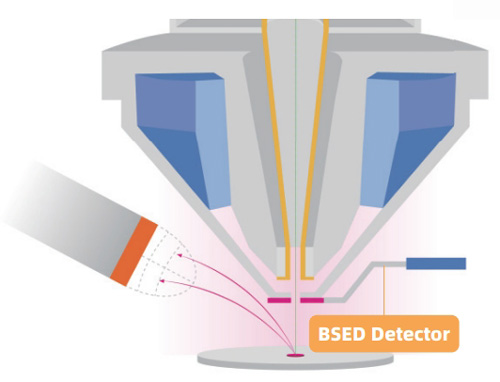
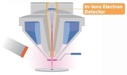
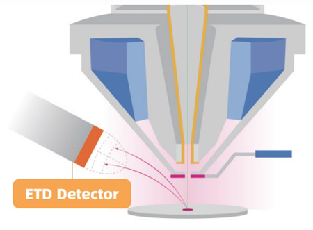
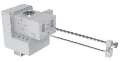
CIQTEK SEM systems support a variety of high-performance detectors and hardware accessories designed to enhance imaging capabilities, streamline workflows, and support advanced applications across materials science, semiconductors, and nanotechnology.
These optional components allow users to tailor their SEM setup to specific analysis needs—whether it’s improving surface contrast, capturing internal structures, or increasing throughput in demanding lab environments.
Scanning electron microscopes (SEMs) are essential tools in research, quality control, and product development across a wide range of industries. Their ability to deliver high-resolution surface and cross-sectional imaging makes them ideal for analyzing materials at the microscale and nanoscale.
Life Sciences – Tissue morphology, cell structures (non-biological SEM only)
Whether you’re in R&D or production, SEMs provide the insight needed to improve processes, validate performance, and drive innovation.
Why Choose JH Technologies for Your Scanning Electron Microscope
For over 35 years, JH Technologies has helped researchers, engineers, and industrial professionals with advanced imaging solutions—and for the past 5 years, we’ve extended that expertise to include high performance, cost-effective scanning electron microscope (SEM) systems.
Our SEM systems deliver exceptional imaging capabilities at the lowest cost of ownership—without compromising quality or performance. As a trusted partner to organizations across North America, we back every system with expert guidance, responsive support, and hands-on service from experienced microscopy specialists.
Whether you’re outfitting a new lab or upgrading your imaging capabilities, JH Technologies is here to help you choose the right SEM, get you up and running quickly, and ensure your lasting success.


