

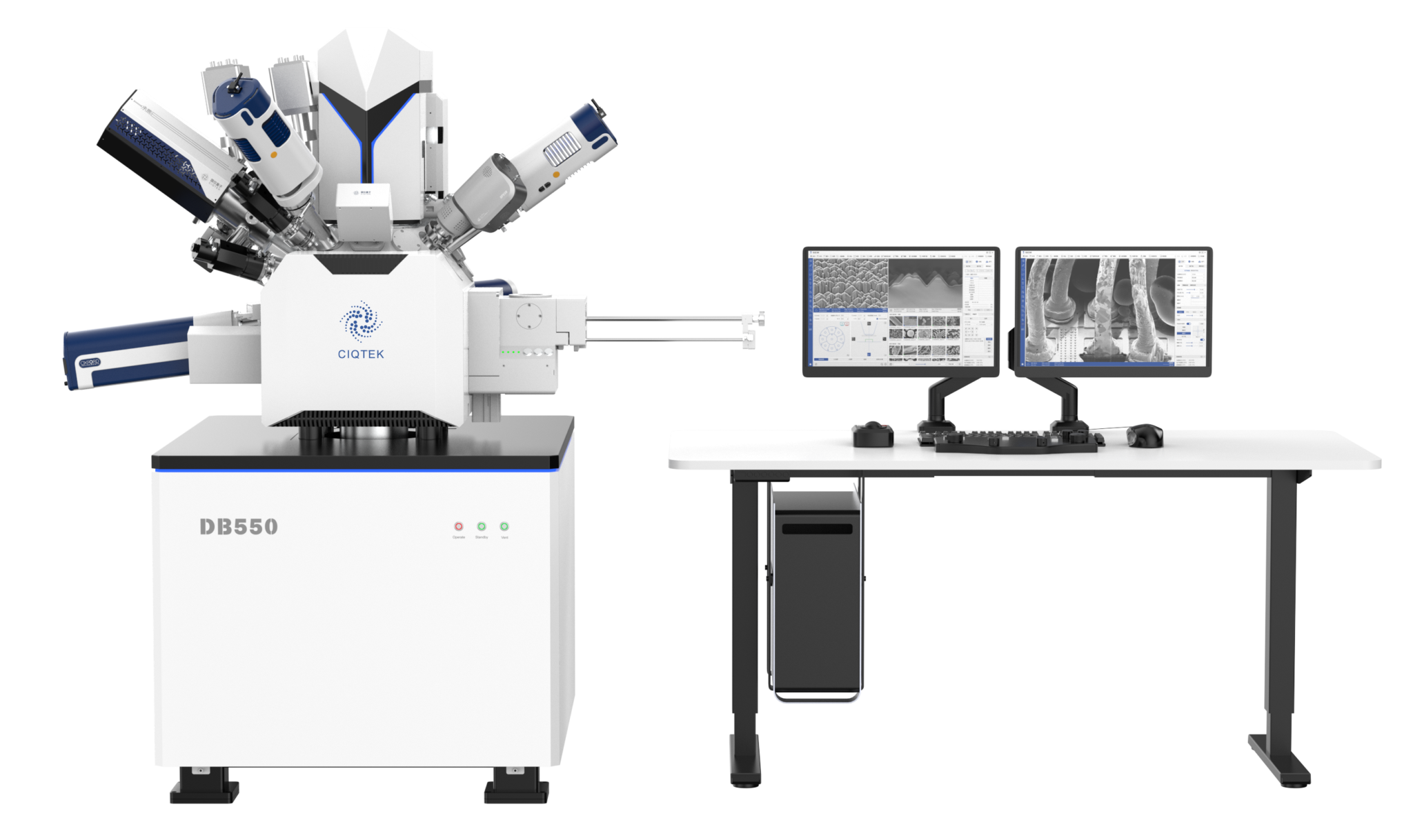
DB550 FIB-SEM (Focused Ion Beam SEM) | High Precision Nano-Analysis
FIB-SEM | Focused Ion Beam Scanning Electron Microscope (New)
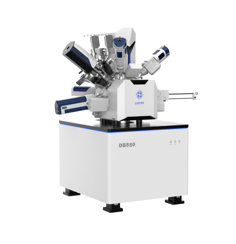
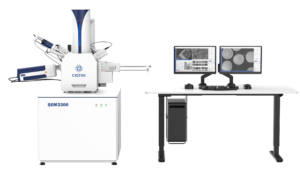
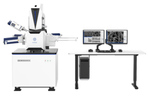
The CIQTEK DB550 is a high-performance Focused Ion Beam SEM (FIB-SEM) system that goes beyond traditional electron microscopy by integrating ion beam processing and nano-analysis capabilities.
A focused ion beam scanning electron microscope (FIB-SEM) combines the precision of a focused ion beam with the high-resolution imaging of a scanning electron microscope in a single integrated system. The result is an instrument capable of simultaneous imaging, milling, cross-sectioning, and nano-fabrication at the nanoscale.
JH Technologies supplies the CIQTEK DB550 FIB-SEM — a high-performance dual-beam system engineered for semiconductor failure analysis, advanced materials research, and nano-analysis applications. With over 35 years of electron microscopy expertise, JH Technologies helps labs across North America select, deploy, and support the right FIB-SEM system for their work.(New)
Keywords: fib sem (720/mo), fib-sem (260/mo), focused ion beam scanning electron microscope (30/mo), fib sem microscope (70/mo)
DB550 FIB-SEM Microscope Key Features
The CIQTEK DB550 FIB-SEM delivers unparalleled resolution and precision with its integrated ion and electron beam technology, making it an essential tool for nanotechnology research and industrial applications.
Reduces spatial charging effects, enhancing low-voltage imaging performance.
Features Ga+ liquid metal ion source with nano fabrication precision down to 3nm resolution.
Three-axis system with 10nm stepper motor accuracy for advanced specimen positioning.
Precisely delivers gases for material modification.
Supports up to 8-inch samples, reducing contamination and improving sample handling efficiency.
Includes Everhart-Thornley Detector (ETD), In-Lens Detector, Back-Scattered Electron Detector (EBSD), and STEM Detector for versatile material characterization.
Optimized for non-conductive and sensitive materials, improving imaging contrast and clarity.
Designed for semiconductors, energy research, materials science, and nanotechnology fabrication.
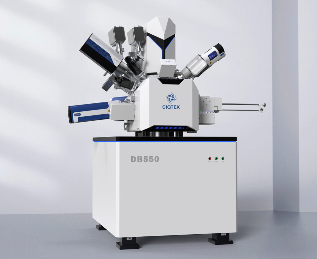
DB550 FIB-SEM Key Features (New)
The CIQTEK DB550 FIB-SEM delivers exceptional resolution and precision by integrating a high-precision gallium ion beam column with advanced electron optics. It is designed for labs that need a reliable, all-in-one focused ion beam system for imaging and nano-fabrication.
Feature accordion items (keep existing expand/collapse structure):
- Super Tunnel Electron Optics Technology — Reduces spatial charging effects, improving low-voltage imaging performance and contrast.
- High-Precision Gallium Ion Beam — Focused ion beam column delivers precise milling, deposition, and cross-sectioning at nanoscale resolution.
- Integrated Nano-Manipulator — Enables in-situ sample manipulation for TEM lamella preparation and targeted material extraction.
- Comprehensive Gas Injection System — Supports gas-assisted etching and deposition for advanced nano-fabrication workflows.
- Specimen Exchange Loadlock — Maintains vacuum integrity during sample exchange, reducing pump-down time and increasing throughput.
- Multi-Mode Advanced Imaging Detectors — Simultaneous fib image acquisition across multiple signal types for comprehensive surface and subsurface analysis.
- Low-Voltage, High-Resolution Imaging — Achieves high-contrast fib sem imaging across a wide voltage range without specimen damage.
- Cross-Industry Application Versatility — Suited for semiconductor, materials science, life science, and advanced manufacturing applications.
Keywords –
fib sem (720/mo), fib system (70/mo), fibsem (70/mo), focused ion beam column (40/mo), fib image (110/mo)
DB550 Focused Ion Beam SEM Performance Advantages
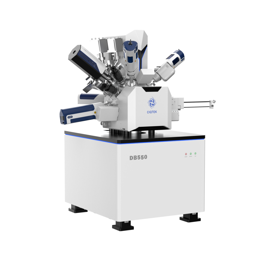
Delivering high-precision nano-fabrication and imaging, the DB550 Focused Ion Beam FIB-SEM Microscope is an essential tool for semiconductor failure analysis, cross-sectioning, and advanced materials research.
- Unmatched Nano-Scale Imaging & Fabrication – Combines high-resolution electron imaging with ion beam milling for precise material modification.
- Cross-Sectioning & TEM Sample Preparation – Enables ultra-thin fabrication for Transmission Electron Microscopy (TEM)
- High-Resolution Imaging Across Multiple Voltage Ranges
- Reduced Spatial Charging Effects – Super tunnel electron optics minimize charging, improving low-voltage imaging contrast.
- Improved Lens Aberration Correction – Enhances clarity and resolution across different imaging modes.
- All-in-One Nano-Analysis & Fabrication Workstation – Integrates gas injection, ion beam milling, and imaging for advanced research.
- Advanced Semiconductor Failure Analysis – Supports defect inspection, circuit modification, and material etching.
Focused Ion Beam SEM Performance Advantages (New)
The DB550 focused ion beam scanning electron microscope is purpose-built for applications where standard SEM imaging is not enough. By integrating ion beam milling with electron beam imaging, it enables workflows that neither instrument can achieve alone — making it the preferred fib sem system for semiconductor failure analysis, cross-sectioning, and advanced materials research.
- Unmatched Nano-Scale Imaging & Fabrication — Combines high-resolution electron imaging with ion beam milling for precise material modification and fib imaging at sub-nanometer scale.
- Cross-Sectioning & TEM Sample Preparation — Enables ultra-thin lamella fabrication for Transmission Electron Microscopy (TEM), with the nano-manipulator for in-situ extraction.
- High-Resolution Imaging Across Multiple Voltage Ranges — Delivers consistent image quality from low-voltage to high-voltage modes, adapting to a wide range of materials.
- Reduced Spatial Charging Effects — Super tunnel electron optics minimize charging artifacts, improving low-voltage imaging contrast on non-conductive samples.
- Improved Lens Aberration Correction — Enhances image clarity and resolution across different imaging modes and voltage settings.
- All-in-One Nano-Analysis & Fabrication Workstation — Integrates gas injection, ion beam milling, and multi-mode imaging in a single fib system footprint.
- Advanced Semiconductor Failure Analysis — Supports defect inspection, circuit modification, material etching, and focused ion beam column work on semiconductor devices.
- Dual Ion Beam Scanning Electron Microscope Architecture — The dual-beam design allows real-time SEM monitoring during FIB milling, enabling precise, damage-free cross-sections.
Keywords –
fib ion (390/mo), dual ion beam scanning electron microscope (210/mo), focus ion beam (110/mo), fib image (110/mo), fib system (70/mo), focused ion beam column (40/mo), plasma fib (40/mo)
FIB-SEM Software Capabilities & Accessories
The DB550 FIB-SEM features a powerful software suite to streamline research and enhance nano-analysis capabilities.
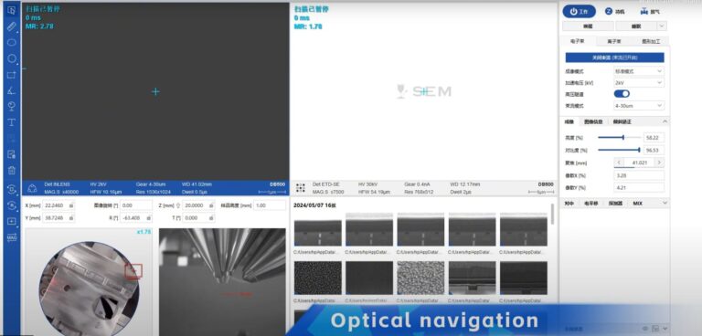
- User-Friendly GUI – Intuitive interface for controlling FIB-SEM functions.
- Specimen Characterization Tools – Comprehensive analysis tools for material science and semiconductor research.
- Cross-Section Analysis Software – Provides detailed structural visualization and precision sectioning controls.
- Compatibility with Multiple Signal Detection Modes
- Micro/Nano Fabrication Support – Includes customizable workflow automation for nano-manufacturing applications.
- Software Development Kit (SDK) Available – Enable custom integration and automation for specialized research workflows.
- Optional Image Post-Processing Tools – Enhances contrast, noise reduction, and feature extraction for high-precision imaging.
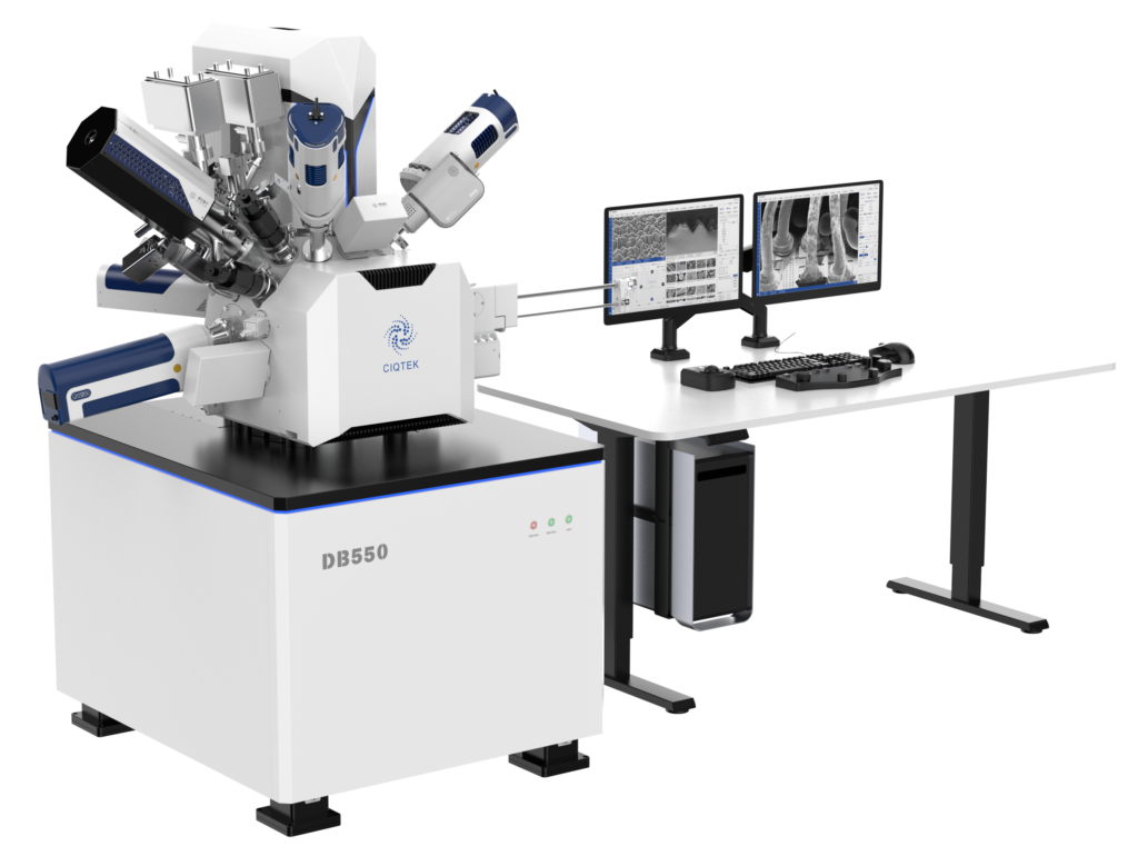
FIB-SEM Software Capabilities & Accessories (New)
The DB550 FIB-SEM includes a comprehensive software suite designed to streamline focused ion beam scanning electron microscope workflows and enhance nano-analysis capabilities across research and industrial environments.
- User-Friendly GUI — Intuitive interface for controlling all FIB-SEM functions, including ion beam, electron beam, and detector settings.
- Specimen Characterization Tools — Comprehensive analysis tools for material science, semiconductor research, and fib imaging services workflows.
- Cross-Section Analysis Software — Provides detailed structural visualization and precision sectioning controls for cross-sectioned samples.
- Compatibility with Multiple Signal Detection Modes — Supports secondary electron, backscattered electron, and STEM detector configurations.
- Micro/Nano Fabrication Support — Customizable workflow automation for nano-manufacturing, including gas-assisted deposition and focus ion beam etching.
- Software Development Kit (SDK) Available — Enables custom integration and automation for specialized research workflows.
- Optional Image Post-Processing Tools — Enhances contrast, noise reduction, and feature extraction for high-precision fib image analysis.
Keywords –
fib imaging services (50/mo), fib image (110/mo), focus ion beam (110/mo), fib-sem (260/mo)
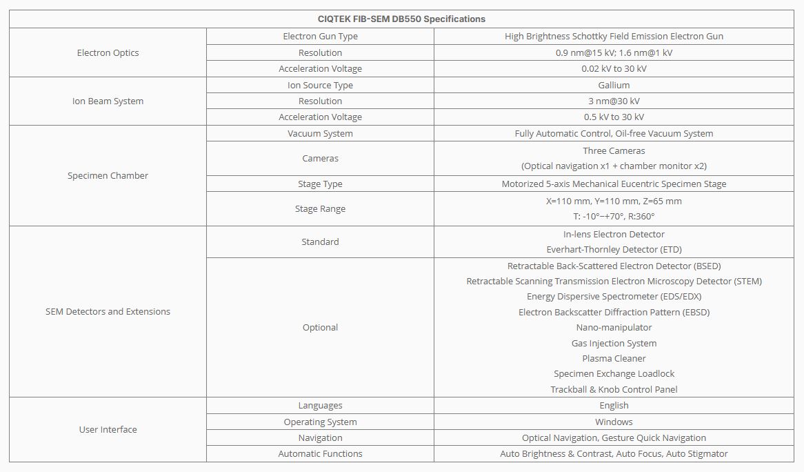
DB550 Focused Ion Beam SEM Specifications
FIB-SEM Videos
Downloads
Related Products
Downloads
FIB-SEM Frequently Asked Questions
What is a FIB-SEM?
A FIB-SEM (Focused Ion Beam Scanning Electron Microscope) is a dual-beam instrument that combines a focused ion beam column with a scanning electron microscope. The ion beam is used for precision milling, deposition, and cross-sectioning, while the electron beam provides high-resolution imaging. Together, they enable nano-scale analysis and fabrication in a single system.
What is the difference between a FIB system and a standard SEM?
A standard scanning electron microscope uses only an electron beam for imaging. A FIB system adds a focused ion beam — typically gallium — that can physically mill, etch, and deposit material on a sample. This makes a FIB-SEM far more versatile for applications like TEM sample preparation, semiconductor failure analysis, and 3D tomography.
What is a dual ion beam scanning electron microscope?
A dual ion beam scanning electron microscope, or dual-beam FIB-SEM, has two columns: one for the electron beam (SEM) and one for the focused ion beam (FIB). This configuration allows real-time SEM imaging while the FIB mills the sample, enabling precise, damage-free cross-sectioning and in-situ analysis.
What are common FIB-SEM applications?
FIB-SEM systems are used across a wide range of fields, including semiconductor failure analysis and circuit edit, TEM and STEM sample preparation, nano-scale materials characterization, 3D tomography and volume imaging, and micro/nano fabrication. The DB550 is designed to support all of these workflows.
Can the DB550 FIB-SEM be used for FIB imaging services?
Yes. JH Technologies also offers FIB imaging services and analytical support through its JH Analytical Services division. Contact us to discuss sample analysis, imaging, or cross-sectioning services if you need results before committing to a system.
🔑 Keywords targeted in this section: fib sem (720/mo), fib-sem (260/mo), fib system (70/mo), dual ion beam scanning electron microscope (210/mo), plasma fib (40/mo), fib imaging services (50/mo), fibsem (70/mo)
Contact Us
The CIQTEK DB550 FIB-SEM is a high-performance focused ion beam scanning electron microscope with a dual-beam architecture. Contact JH Technologies for a detailed quote or to discuss configuration options for your application.”
Get Your Free Price Quote