
Tariff Policy Simplified: Stability, Transparency, and Trust
Recent Blogs JHT Tariff Policy: Stability, Transparency, and Trust Stability,

Demonstration Equipment: Beating The Tariff Trap
Recent Blogs Demonstration Equipment: Beating the Tariff trap In a
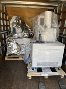
The Case of the Missing SEMs: A Story of Quick Thinking, Teamwork & Tech Recovery
Recent Blogs The Case of the Missing SEMs: A Story

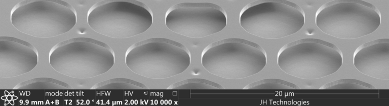
JH Technologies Partners with Xavis to Deliver Advanced Inspection Solutions to North America
Recent Blogs JH Technologies Partners with Xavis to Deliver Advanced
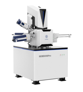
New JH Technologies Partnership Focuses on Scanning Electron Microscopes
Recent Blogs New JH Technologies Partnership Focuses on Scanning Electron
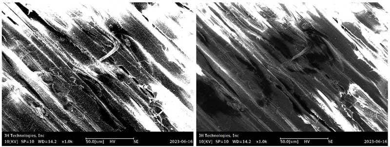
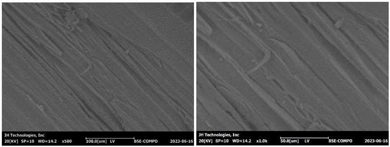
However, when imaged under low-vacuum conditions, the pine wood sample exhibits no charge accumulation, resulting in improved contrast and finer details, thanks to the application of a higher energy 20kV beam and reduced charge accumulation.
Need Help? Complete the form on this page, and a JH team member will be in touch.