Recent Blogs

What Happens When Elves Discover Surface Metrology?
Recent Blogs What Happens When Elves Discover Surface Metrology? Candy

2025 Equipment Tax Benefits to Consider
Recent Blogs Equipment Tax Benefits for 2025! Is Now the
Reviving Legacy AFMs: How to Unlock New Capabilities
Recent Blogs Reviving Legacy AFMs: How to Unlock New Capabilities

Automotive Paint Layer Analysis with Microscopy & EDS | JH Technologies
Recent Blogs Automotive Paint Layer Analysis with Optical Microscopy, SEM,
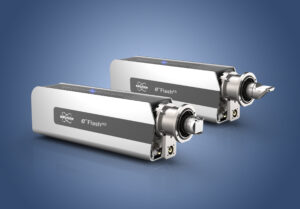
What Is EBSD? A Guide to Electron Backscatter Diffraction in SEM
Recent Blogs A Guide to Electron Backscatter Diffraction (EBSD) Electron
A Guide to Electron Backscatter Diffraction (EBSD)
Electron Backscatter Diffraction (EBSD) is a powerful technique used in conjunction with scanning electron microscopy (SEM) to analyze the crystallographic structure of materials. Widely used in materials science, metallurgy, geology, and semiconductor research, EBSD provides detailed insights into grain structure, phase distribution, and orientation.
In this brief guide, we’ll explain what EBSD is, how it works, and what makes it such a valuable tool for materials analysis.
What is EBSD?
EBSD is a microanalytical technique that uses the interaction of an electron beam with a crystalline sample inside a scanning electron microscope. When the beam strikes a tilted (typically ~70°), polished sample surface, it produces Kikuchi diffraction patterns that reveal critical information about the material’s internal structure.
These patterns are then indexed against crystallographic databases to generate orientation imaging maps (OIM), inverse pole figures, pole figures, and misorientation analyses.
An EBSD system typically includes:
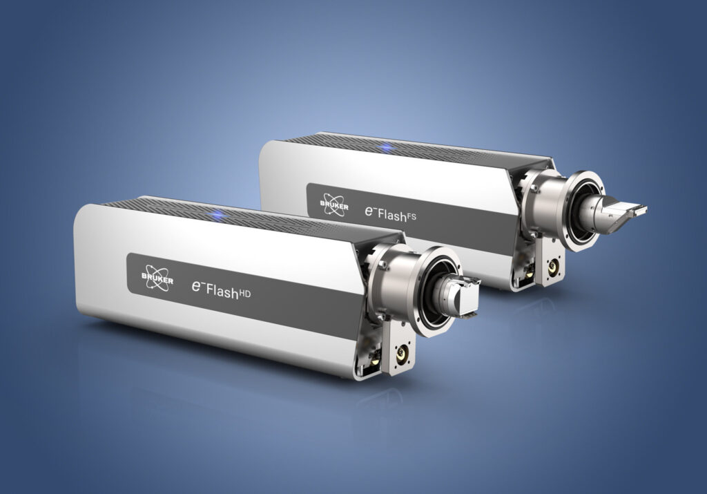
- A high-sensitivity detector (camera or phosphor screen)
- Diffraction pattern acquisition hardware
- Analysis software
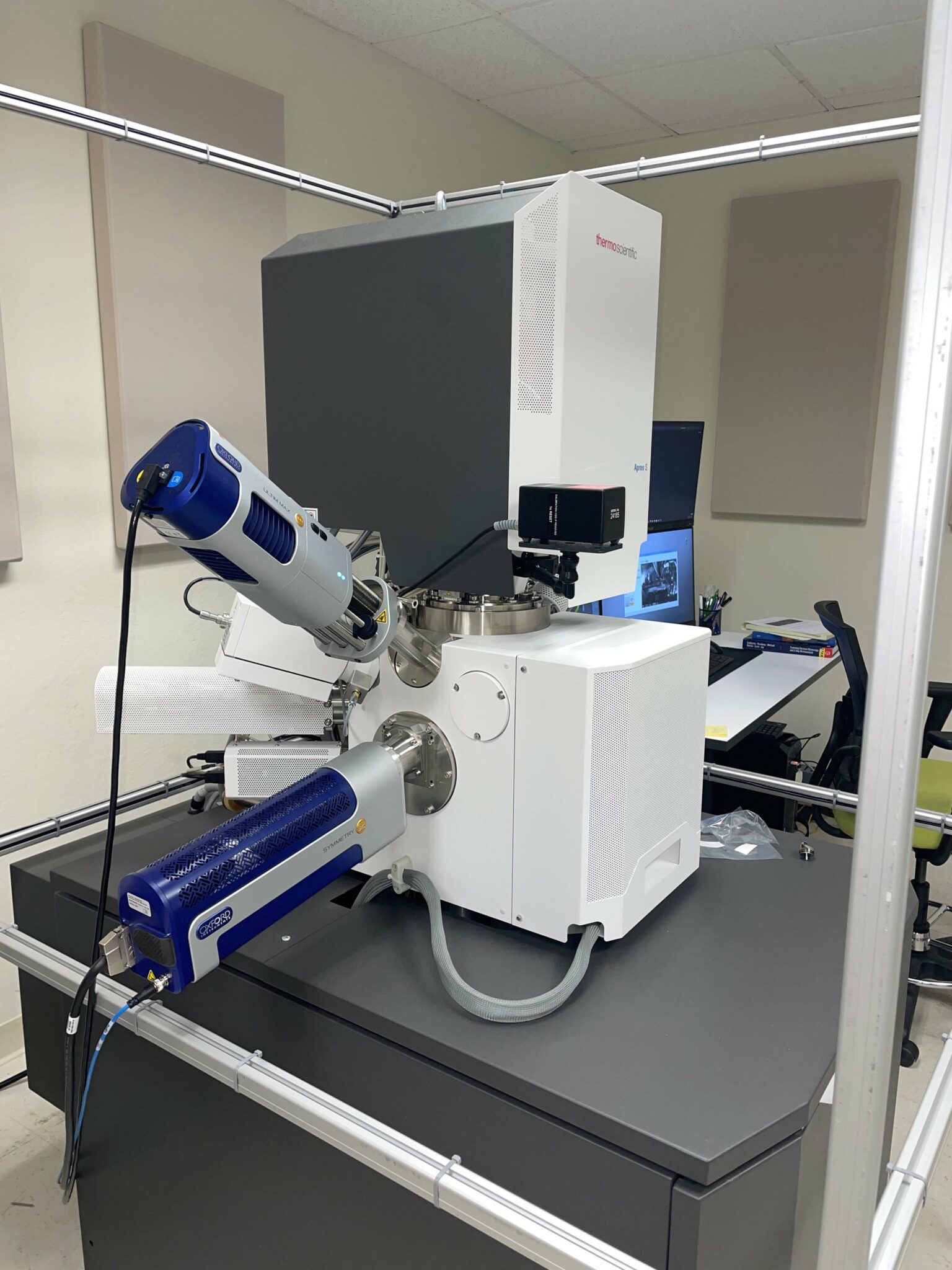
- Integration with an SEM platform
Researchers and engineers use the EBSD technique to identify crystallographic orientation, map grain boundaries, detect phase composition, and study deformation, strain, and recrystallization.
How Does EBSD Work?
Here’s a step-by-step overview of the EBSD process:
Step 1 – Sample Preparation
High-quality sample preparation is essential for reliable EBSD results. The sample surface must be extremely flat and clean to allow clear diffraction patterns to form. Typically, this involves mechanical polishing followed by final cleaning with chemicals or ion milling to remove surface damage.
Need help with prep? Read our guide to EBSD sample preparation.
Step 2 – SEM Setup and Sample Tilt
EBSD is performed using a scanning electron microscope. The sample is mounted and tilted—usually at a 70-degree angle—to increase the number of backscattered electrons to diffract. This geometry improves the quality and intensity of the patterns detected.
Step 3 – EBSD Pattern Formation
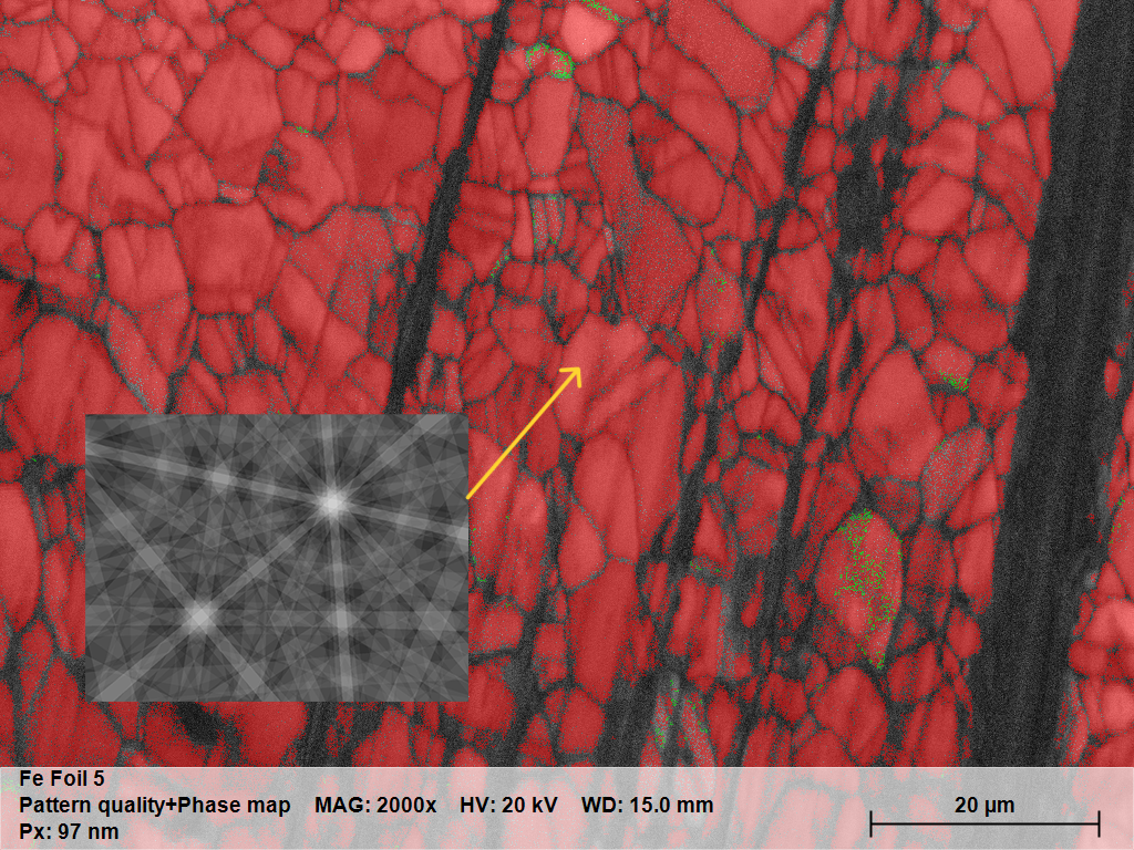
When the electron beam hits the tilted sample, it generates an Electron Backscatter Diffraction Pattern (EBSP). These patterns contain Kikuchi bands, which correspond to the atomic planes within the crystal.
Step 4 – Pattern Capture and Analysis
A phosphor screen or camera captures the EBSP. Advanced EBSD software then indexes these patterns, identifying the orientation of individual grains and reconstructing the material’s microstructure in detailed maps.
EBSD analysis can reveal critical crystallographic information, such as:
- Recrystallization and grain growth kinetics
- Twin boundary identification and quantification
- Phase transformation mapping
- Residual strain and local misorientation assessment
- Texture evolution in additive manufacturing and thermomechanical processes
Step 5 – Data Interpretation
The final output includes:
- Orientation maps
- Phase distribution
- Grain boundary characterization
- Texture and misorientation analysis
These results are essential for understanding a material’s behavior under stress, during processing, or in failure conditions.
Why EBSD Matters
EBSD enables non-destructive, high-resolution crystallographic analysis directly within your SEM workflow. It’s particularly valuable for:
- Improving mechanical property predictions
- Evaluating heat treatment effects
- Supporting failure analysis in metals and ceramics
- Conducting advanced research in nanomaterials and semiconductors
And with modern tabletop SEMs like the Coxem EM-40, EBSD is now more accessible and affordable than ever before.
Learn More
Want to bring EBSD capabilities into your lab or QA environment?
Explore our EBSD systems for SEM or contact our team to request a quote or schedule a demo.

