Affordable EBSD (electron Backscatter Diffraction) for Material Analysis

ebsd analysis grain map

EBSD is a powerful analytical technique used to examine the crystallographic structure of materials.

The Only Small-footprint SEM with EBSD Capabilities

Experience the cutting-edge capabilities of our reliable and affordable Electron Backscatter Diffraction (EBSD) system integrated with a compact tabletop scanning electron microscope (SEM). Discover how our advanced EBSD and EDS features can improve your material analysis with a free demo.

ebsd on small sem

Reliable And Affordable Analysis

The Coxem EM-40 delivers full analytical power, covering more than 95% of typical applications. This compact yet powerful system includes fully integrated EBSD and EDS capabilities, all managed seamlessly with Bruker Esprit software.

  • Crystallographic Texture Analysis—Conduct orientation distribution and texture analysis to explore the crystallographic texture of your materials.
  • Quantitative Microstructure Analysis—Utilize subsetting to perform detailed quantitative analysis of microstructures.
  • Grain Boundary Analysis—Gain insights into grain boundary characteristics, crucial for understanding material properties and performance.
  • Automatic Grain Size and Shape Distribution—Automate the analysis of grain size and shape distribution for more efficient and accurate studies.
  • Phase Identification and Distribution—Accurately identify and map different phases within your sample, providing a deeper understanding of material composition.
  • Correlated Chemical and Crystallographic Results—Achieve a comprehensive view of your material by correlating chemical composition with crystallographic orientation and structure.
  • User-Friendly Design—The simple and intuitive design ensures low downtime and minimal cost of ownership, making advanced material analysis accessible and affordable.

What is Electron Backscatter diffraction (EBSD)?

EBSD is a scanning electron microscopy (SEM) technique that analyzes diffraction patterns of electrons from a crystalline sample. Scientists commonly use this technique in material science, metallurgy, geology, and engineering.

An EBSD system consists of equipment and software integrated with an SEM.

How does it work?

Here’s a brief overview of how EBSD works:

Step 1 – Sample Preparation

To achieve accurate results, meticulous sample preparation is crucial. The sample surface must be extremely flat and clean to allow for accurate diffraction pattern formation. This method uses machines to polish and create a smooth surface. After that, we use chemicals or ions to remove any remaining damage or dirt.

Read our article about the best method to prepare a sample for EBSD.

Step 2 – SEM Integration

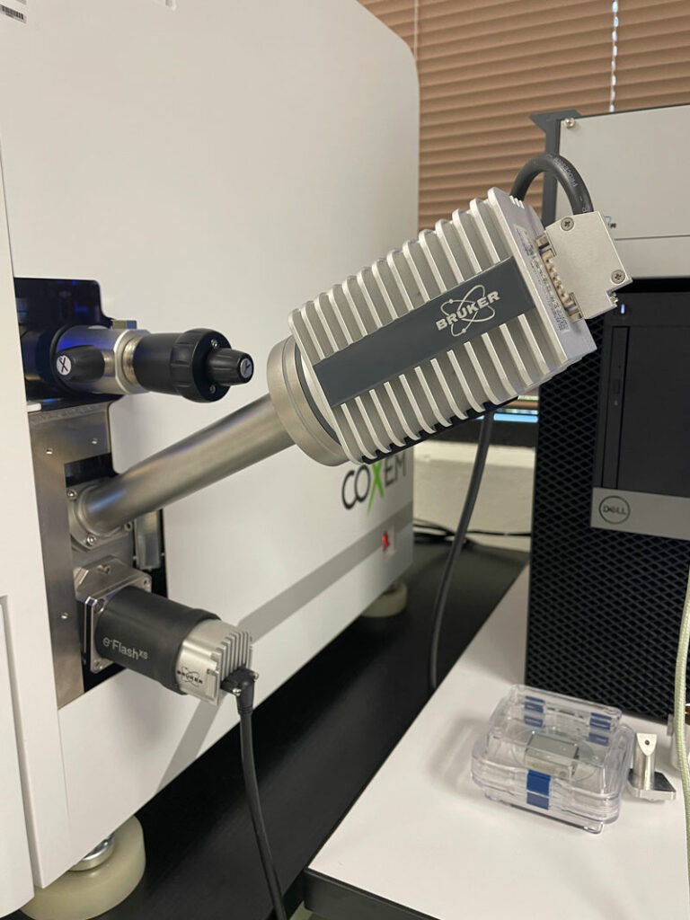
Researchers perform EBSD using a Scanning Electron Microscope (SEM). Typically, the sample tilts at a 70-degree angle to the electron beam. This tilt helps produce high-quality diffraction patterns. It does so by increasing electron backscattering.

Step 3 – Diffraction Results

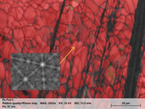
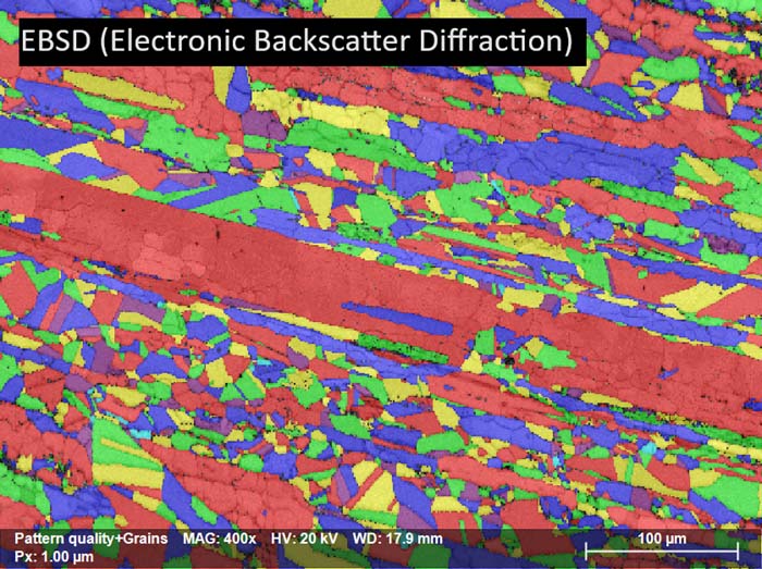
When the electron beam hits the tilted sample, it makes an Electron Backscatter Diffraction Pattern (EBSP). This pattern, featuring Kikuchi bands, represents the crystal’s crystallographic planes.

Step 4 – Diffraction Analysis

A phosphor screen or a high-sensitivity camera captures the EBSP. Specialized software analyzes these patterns to determine the crystal grains’ orientation, indexing the Kikuchi bands to specific crystallographic orientations and creating detailed microstructure maps.

Step 5 – Analyzed Data

The analyzed data provides comprehensive information on the crystallographic orientation, phase distribution, and texture. Maps and figures present this data, helping us understand properties, mechanisms, and processes.

Top 3 Advantages of EBSD on a Tabletop SEM

EBSD has many benefits for analyzing materials, making it a valuable tool in different scientific and industrial settings. However, in the past, EBSD was only available on floor-standing SEMs and was also quite costly to add. Customers typically see costs from $750K to over $1 million.

Today, Bruker has created a compact and cost-effective EBSD detector that fits on the Coxem EM30 and EM40 table SEMs. Its cost ranges from $185K to $220K. This detector offers huge potential savings while providing significant analysis capability.

Here are the main advantages of using EBSD:

  1. High-resolution and precise material characterization—Provides detailed analysis of crystallographic structures, essential for understanding grain size, shape, and orientation.
  2. Non-destructive testing capabilities—Allows repeated analyses without altering or damaging the sample.
  3. Versatility—Suitable for various materials, including metals, ceramics, minerals, and composites.