Skip to content
Product Groups
Microscopes
Ergonomic Routine Stereo Microscopes
Routine Inspection/Assembly Microscopes
Ergonomic Research Stereo Microscopes
Stereo Microscope Lighting
Compound Upright Microscopes
Compound Microscopes Inverted
Education
Forensics
Digital
SEM & Accessories
Electron Microscopy Sample Preparation
High Resolution SEM
Tabletop & Compact Floor Standing SEM
SEM Detector Software & Hardware
Sample Prep & Cross-sectioning
Hardness Testing
Metrology & 3D Characterization
Cameras, Software & Lenses
Accessories and Lenses
X-Ray Imaging
Analytical Services
Applications
Microtechnology
Medical Device
Metallography
Material Science
Education
Semiconductor
Sample Preparation for Electron Microscopy
Forensics
Customer Support
Promotions
About Us
About JH
Events
Blogs & Updates
JH Newsletter
Careers
iFUSE
Shop
Search
Product Search
Product Groups
Microscopes
Ergonomic Routine Stereo Microscopes
Routine Inspection/Assembly Microscopes
Ergonomic Research Stereo Microscopes
Stereo Microscope Lighting
Compound Upright Microscopes
Compound Microscopes Inverted
Education
Forensics
Digital
SEM & Accessories
Electron Microscopy Sample Preparation
High Resolution SEM
Tabletop & Compact Floor Standing SEM
SEM Detector Software & Hardware
Sample Prep & Cross-sectioning
Hardness Testing
Metrology & 3D Characterization
Cameras, Software & Lenses
Accessories and Lenses
X-Ray Imaging
Analytical Services
Applications
Microtechnology
Medical Device
Metallography
Material Science
Education
Semiconductor
Sample Preparation for Electron Microscopy
Forensics
Customer Support
Promotions
About Us
About JH
Events
Blogs & Updates
JH Newsletter
Careers
iFUSE
Shop
Blogs: Latest News, Updates, Tech Notes
Latest
SEM
Sample Prep
Metrology
Microscopy
Education
Leica
JH
What Happens When Elves Discover Surface Metrology?
December 16, 2025
2025 Equipment Tax Benefits to Consider
October 14, 2025
Reviving Legacy AFMs: How to Unlock New Capabilities
September 17, 2025
Automotive Paint Layer Analysis with Microscopy & EDS | JH Technologies
September 8, 2025
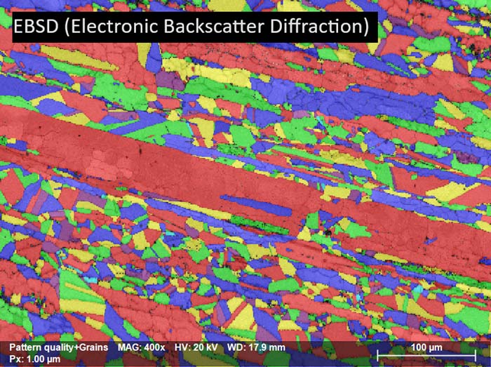
What Is EBSD? A Guide to Electron Backscatter Diffraction in SEM
August 26, 2025
What is Ion Milling?
August 26, 2025
EBSD Analysis and SEM Platform Considerations
August 11, 2025
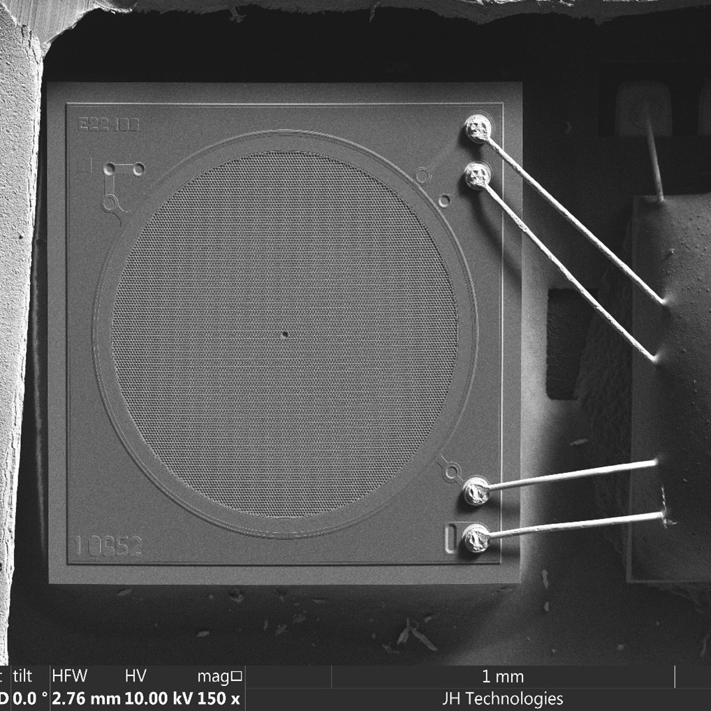
SEM Images Gallery
August 6, 2025
Multi-Technique Characterization of Solder Balls
August 6, 2025
Precision Solder ball Analysis Using Ion Beam Polishing and SEM
July 1, 2025
Tariff Policy Simplified: Stability, Transparency, and Trust
April 15, 2025
Demonstration Equipment: Beating The Tariff Trap
April 15, 2025
The Case of the Missing SEMs: A Story of Quick Thinking, Teamwork & Tech Recovery
April 15, 2025
JH Technologies Partners with Xavis to Deliver Advanced Inspection Solutions to North America
January 16, 2025
New JH Technologies Partnership Focuses on Scanning Electron Microscopes
January 9, 2025
Lithium Battery Sample Preparation
May 16, 2024
What is the best method to prepare a sample for EBSD? [Application Note]
May 16, 2024
What is the best way to preserve and transport polished samples?
May 16, 2024
Handling Delicate Samples [Tips ‘n Tricks]
May 16, 2024
Sample Polishing Methods: Diamond Grinding Disks [APPLICATION NOTE]
May 16, 2024
Polishing Soft Materials: What is the Best Way?
May 16, 2024
Memory Device Cross-Sectioning [Learn from the JHA Team]
May 16, 2024
How To Choose The Correct Mounting Method And Epoxy For Your Samples
May 16, 2024
What does a heat-treated metal look like after sample preparation and etching?
May 16, 2024
Application Note: Proper Maintenance and Cleaning of your Sputter Coater
May 16, 2024
Solutions for Semiconductor Applications
May 16, 2024
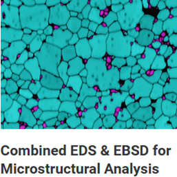
Bruker EDS & EBSD
May 16, 2024
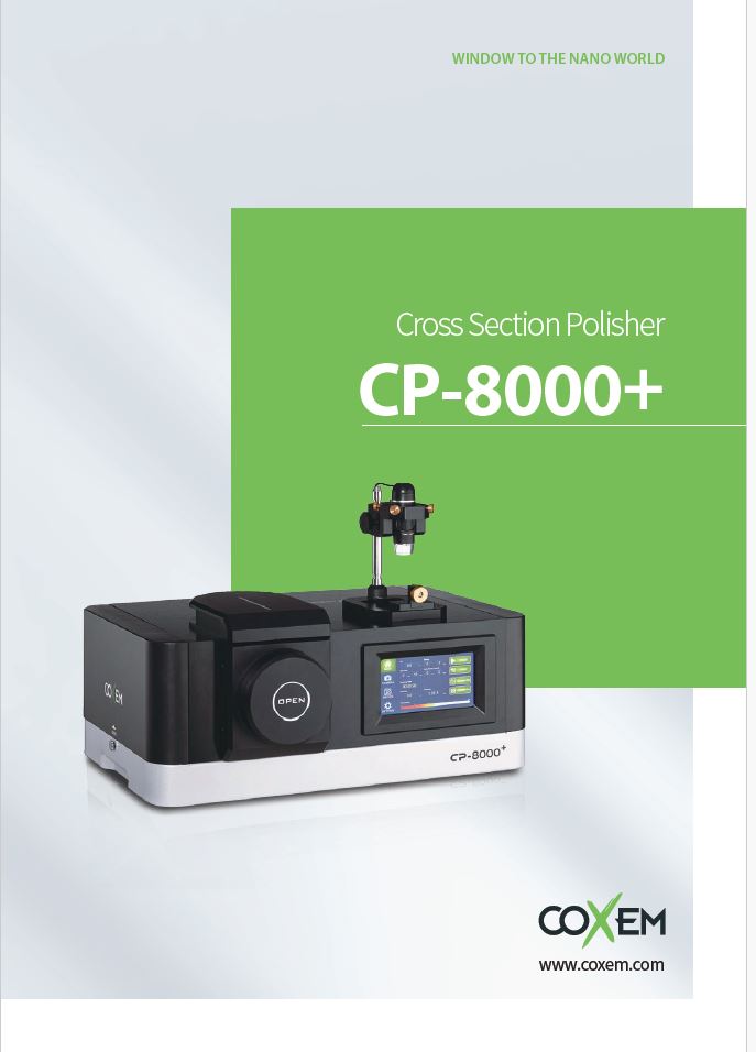
Coxem CP-8000
May 16, 2024
Product Groups
Microscopes
Ergonomic Routine Stereo Microscopes
Routine Inspection/Assembly Microscopes
Ergonomic Research Stereo Microscopes
Stereo Microscope Lighting
Compound Upright Microscopes
Compound Microscopes Inverted
Education
Forensics
Digital
SEM & Accessories
Electron Microscopy Sample Preparation
High Resolution SEM
Tabletop & Compact Floor Standing SEM
SEM Detector Software & Hardware
Sample Prep & Cross-sectioning
Hardness Testing
Metrology & 3D Characterization
Cameras, Software & Lenses
Accessories and Lenses
X-Ray Imaging
Analytical Services
Applications
Microtechnology
Medical Device
Metallography
Material Science
Education
Semiconductor
Sample Preparation for Electron Microscopy
Forensics
Customer Support
Promotions
About Us
About JH
Events
Blogs & Updates
JH Newsletter
Careers
iFUSE
Shop
{"field_798bfda":{"display_mode":"show","fire_action":"All","file_types":"png","logic_data":[{"cfef_logic_field_id":"field_f447988","cfef_logic_field_is":"==","cfef_logic_compare_value":"Yes","_id":"106ced0"}]},"field_94cd4db":{"display_mode":"show","fire_action":"All","file_types":"png","logic_data":[{"cfef_logic_field_id":"field_d910443","cfef_logic_field_is":"==","cfef_logic_compare_value":"Yes","_id":"36b9b61"}]}}
Company
First Name
Last Name
Email
Zip Code
Phone
How can we help you?
I would like a price quote?
Yes
No
Enter Product Name
Do you want to Schedule a demo?
Yes
No
Schedule Date
Submit
Schedule Date
Preferred Time
Company
First Name
Last Name
Email
Phone
Description
Submit
Insert/edit link
Close
Enter the destination URL
URL
Link Text
Open link in a new tab
Or link to existing content
Search
No search term specified. Showing recent items.
Search or use up and down arrow keys to select an item.
Cancel