Equipment End of Life Announcements: Buehler & Leica
Recent Blogs Equipment End-of-Life Announcements: Buehler & Leica Buehler MiniMet
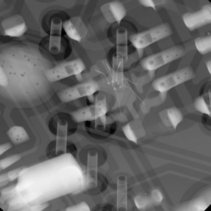
Cone Beam CT vs. Oblique CT: Choosing the Right X-Ray Inspection Technique for 3D Analysis
Recent Blogs Cone Beam CT vs. Oblique CT: Choosing the
Compact vs. High-End EBSD Systems: A Performance Comparison of Detector Technologies
Recent Blogs Compact vs. High-End EBSD Systems: A Performance Comparison

SEM: Low Vaccuum vs. High Vacuum Imaging – Webinar
Recent Blogs 5 Key Takeaways from Our Webinar: Low Vacuum

What Happens When Elves Discover Surface Metrology?
Recent Blogs What Happens When Elves Discover Surface Metrology? Candy