

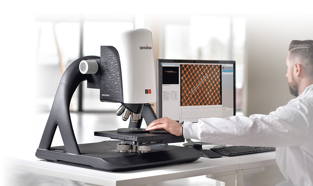
3D Optical Profilometers & Non-Contact Surface Profilers
Optical profilometers, also called 3D surface profilers or non-contact surface profilometers, deliver nanometer-resolution surface measurements without ever touching your sample.
From semiconductor wafers and medical devices to aerospace coatings and automotive textures, Sensofar’s 3D optical profilometers provide the precision and speed modern inspection demands.
What is a 3D Optical Profilometer?
A 3D optical profilometer is a non-contact instrument that uses light to capture high-resolution 3D surface topography without touching the sample. Unlike stylus profilometers, optical systems safely measure delicate, soft, or highly polished surfaces without risk of damage or contamination.
Modern optical profilometers combine multiple technologies in one platform, including:
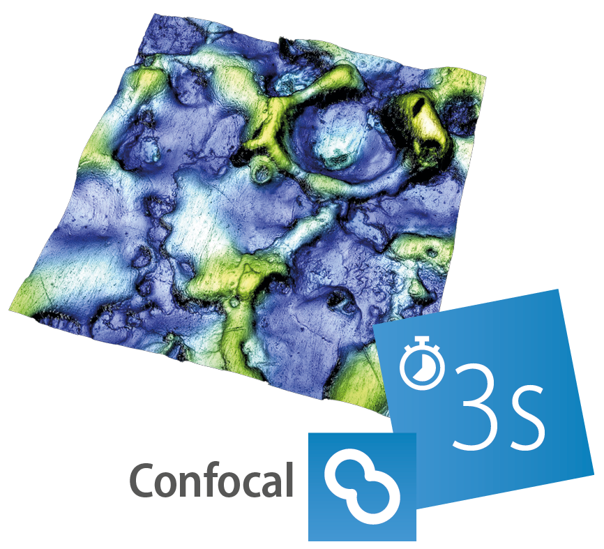
- Confocal microscopy for high-resolution surface analysis
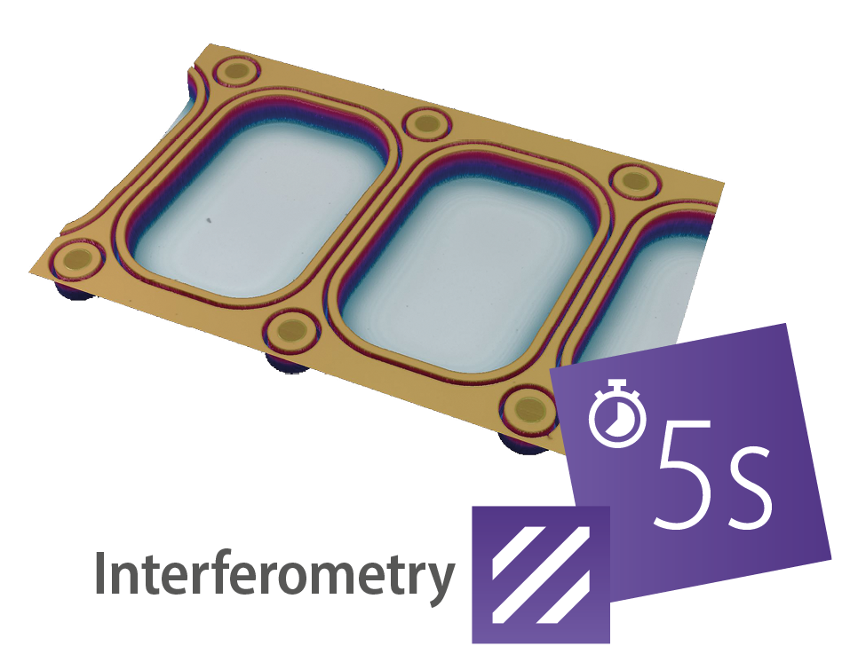
- White Light Interferometry (WLI) for sub-nanometer vertical resolution
- Focus Variation for steep slopes and rough surfaces
- Thin-film measurement for coatings and transparent layers
These optical surface profilers with a multi-technology approach means a single instrument can handle the full range of surface texture measurement challenges across research, quality control, and high-throughput production environments.
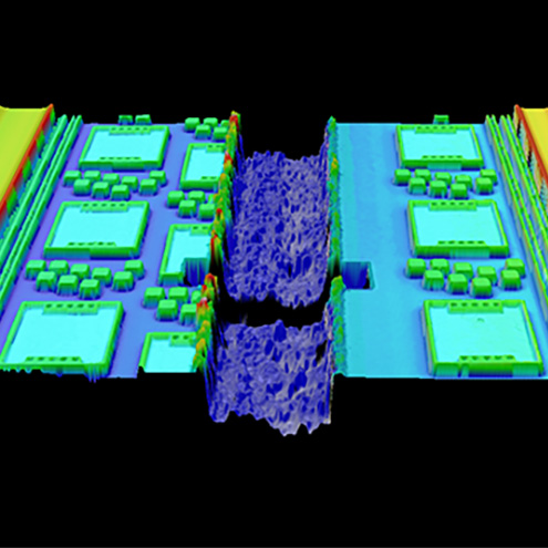
Optical Profilometer vs. Contact (Stylus) Profilometer
Choosing between an optical profilometer and a contact profilometer depends on your application, sample type, and throughput needs. Here’s how they compare:
Optical / Non-Contact Profilometer | Contact / Stylus Profilometer |
No sample contact — safe for delicate surfaces | Stylus touches sample — risk of scratching or damage |
Full 3D areal surface measurement in seconds | 2D line scan only — slow and limited coverage |
Multiple technologies in one system | Single measurement principle — limited flexibility |
Suitable for soft, polished, and thin-film surfaces | Not suitable for very soft, sticky, or contamination-sensitive samples |
High throughput — ideal for production QC | Low throughput — better for simple lab measurements |
ISO 25178 areal parameters as standard output | Limited to ISO 4287 profile parameters |
Sensofar Surface Profilometer Models
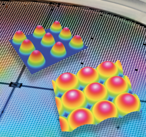
Sensofar offers a complete range of 3D optical surface profilers — from high-resolution research instruments to large-area scanners and fully automated inline systems. All models are available with local support, demo availability, and fast delivery.
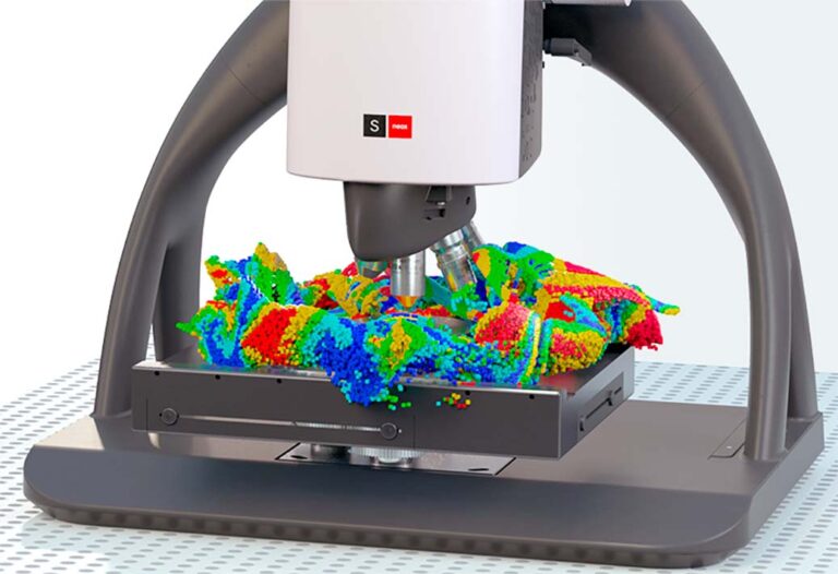
S neox is the most versatile non-contact surface profilometer on the market. Combines confocal, interferometry, focus variation, and thin-film measurement in one system.
- 4 technologies in 1 — no need for multiple instruments
- Sub-nanometer vertical resolution in interferometry mode
- Wide range of microscope objectives for any magnification need
- Ideal for semiconductor, medical device, and research applications
ISO 25178 compliant areal surface texture output
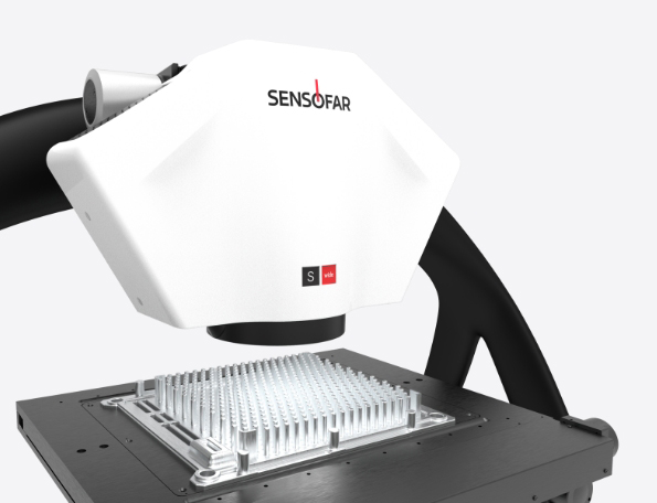
S wide engineered for samples requiring large field-of-view surface measurement without sacrificing resolution or speed.
- Large area scanning with high lateral resolution
- Fast acquisition for production-ready throughput
- Motorized XY stage for extended area mapping
- Ideal for PCBs, displays, solar panels, and large industrial components
S lynx 2 is a compact, portable surface profiler for labs where space and flexibility matter.
- Compact design — for small parts needing high resolution measurement
- Confocal or interferometry technologies
- Ideal for manufacturing, R&D labs, and failure analysis
- Intuitive operation — minimal training required
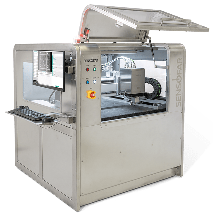
Grand Format built for automated, high-throughput surface inspection on production lines.
- Designed for seamless integration into production environments
- Automated measurement with minimal operator intervention
- Real-time surface quality feedback for process control
- Ideal for semiconductor fabs and high-volume manufacturing
Not sure which system fits your application? Talk to a Surface Metrology Specialist
Benefits of 3D optical profilometers
- Non contact to protect sensitive surfaces
- Nanometer-scale precision
- True 3D surface data-measures full surface topography not just 2D line profiles
- Versatility across materials – works on metals, semiconductors, glass, polymers, coatings, and more.
- Capable of handling any sample size
- Fast, high-throughput inspection-rapid measurements support research and production environments
Is a 3D Optical Profilometer Right for You?
Best fit if:
- You measure delicate or polished surfaces
- You need nanometer scale accuracy
- Your parts have complex geometries
- You require full 3D surface data
- You need fast, repeatable measurments
- Your industry demands tight tolerances such as semiconductor, medical device, aerospace, automotive, or precision manufacturing
Request 3D Optical Profilometer Pricing
Pricing for 3D optical profilometers depends on the measurement requirements, sample type, resolution, automation needs, and system configuration. Our technical specialists will help identify the right Sensofar solution for your application and provide a tailored quote
Contact us to learn which options are right for your application.
3D Optical Profilometer Video
Industries We Serve
Semiconductor & Microelectronics
Sensofar optical profilometers are trusted across semiconductor fabs for wafer surface inspection, thin-film characterization, and process control. The S neox and S mart 2 are particularly well-suited for high-throughput environments where speed and repeatability are critical.
- Wafer surface roughness and flatness measurement
- Thin-film and coating thickness analysis
- Bump, via, and interconnect characterization
- CMP process monitoring and endpoint detection
Medical Devices
Surface finish is a critical quality parameter in medical device manufacturing — from stent inspection to orthopedic implant characterization. Sensofar systems deliver ISO 25178-compliant surface texture measurement required in medical device QC and FDA submissions.
- Stent surface inspection and dimensional verification
- Orthopedic implant surface finish measurement
- Catheter and needle tip characterization
- ISO 25178 areal surface texture compliance
Aerospace & Defense
Aerospace manufacturers rely on precise surface texture measurement equipment to ensure component performance, fatigue life, and compliance with tight specifications. Sensofar surface profilers measure turbine blades, coatings, and composite structures with sub-nanometer precision.
- Turbine blade and engine component surface analysis
- Thermal barrier coating characterization
- Fatigue and wear surface analysis
- Composite material surface texture inspection
Automotive
From cylinder bores to gear surfaces, automotive manufacturers use Sensofar 3D surface profilers to verify surface quality meets tight functional tolerances — ensuring performance, fuel efficiency, and component longevity.
- Cylinder bore and piston surface finish measurement
- Gear and brake component surface texture analysis
- Fuel injector nozzle tip inspection
- Body panel coating and surface roughness verification

Research & Academia
Research institutions and universities across the USA use Sensofar optical profilers for materials science, tribology, biology, and nanotechnology research — where measurement accuracy and flexibility are paramount.
- Materials characterization and surface science
- Tribology, friction, and wear surface studies
- MEMS and nanotechnology device measurement
- Biology and biomaterial surface analysis
Request a Surface Profilometer Quote or Demo
Ready to see what a Sensofar 3D optical profilometer can do for your process? Whether you are evaluating options, planning a budget, or ready to purchase, the JH Technologies team is here to help.
We offer live demos with your own samples, application-specific guidance, and competitive pricing as the exclusive USA distributor for Sensofar. Reach out today to speak with a surface profilometer specialist.
Optical Profilometer FAQs
Before you invest in a surface profilometer, it’s natural to have questions. Below, we’ve answered some of the most common inquiries about surface profilometer capabilities, pricing, features, and use cases to help guide your decision-making process.
Confocal profilometers use a pinhole aperture to reject out-of-focus light, delivering high lateral resolution and the ability to measure steep slopes — ideal for rough or complex surfaces. White Light Interferometers (WLI) use interference fringe analysis to achieve sub-nanometer vertical resolution on smooth, flat surfaces. The Sensofar S neox combines both technologies in a single system, letting you select the best technique for each measurement.
Optical surface profilometers can measure metals, ceramics, polymers, semiconductors, glass, thin films, and biological samples. They are particularly well-suited for smooth, polished, or delicate surfaces where contact measurement would risk damage. For very steep or rough surfaces, focus variation technology extends measurement capability significantly.
In interferometry mode, the Sensofar S neox achieves sub-nanometer vertical resolution — as low as 0.1 nm — making it one of the highest-resolution non-contact surface profilometers available on the market.
Yes. All Sensofar surface profilometers output areal surface texture parameters fully compliant with ISO 25178 — the international standard for 3D surface texture measurement. This is a key requirement in medical device QC, aerospace specifications, and semiconductor process control
Optical profilometers typically range from $80,000 to $250,000+ depending on the model, configuration, objectives, and software selected. Contact JH Technologies for a quote based on your application.
Absolutely. JH Technologies maintains demo centers in Fremont CA, Irvine CA, Portland OR, and Boston MA. You are welcome to bring your own samples for a live measurement demonstration with a Sensofar application specialist. Contact us to schedule your demo.
Yes, Sensofar publishes a handbook on surface profiling you can download it here. Surface profiling handbook