Cone Beam CT vs. Oblique CT: Choosing the Right X-Ray Inspection Technique for 3D Analysis
Recent Blogs Cone Beam CT vs. Oblique CT: Choosing the
Compact vs. High-End EBSD Systems: A Performance Comparison of Detector Technologies
Recent Blogs Compact vs. High-End EBSD Systems: A Performance Comparison

SEM: Low Vaccuum vs. High Vacuum Imaging – Webinar
Recent Blogs 5 Key Takeaways from Our Webinar: Low Vacuum

What Happens When Elves Discover Surface Metrology?
Recent Blogs What Happens When Elves Discover Surface Metrology? Candy

2025 Equipment Tax Benefits to Consider
Recent Blogs Equipment Tax Benefits for 2025! Is Now the
Introduction
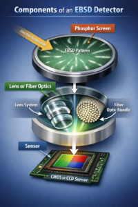
An EBSD detector usually consists of the following components: a phosphor screen (scintillator), lens or fiber optics, and a sensor. The phosphor screen converts the electron signal to a photon signal (Kikuchi pattern). The lens focuses the light into the sensor, and the sensor detects and records the photon signal.
Over the past several decades, EBSD development has focused on speed and signal sensitivity, with one of the improvements being the development of direct electron detection. Direct electron detection technology allows backscattered electrons to be collected directly by the pixelated image sensor without a scintillator, avoiding additional conversion of electrons into photons before collection. With direct electron detection, faster EBSD data collection is possible.
Bruker is one of the world’s leading manufacturers of EBSD detectors, offering a wide range of detectors for different applications. In this paper we examine two different EBSD detectors to show the similarities and differences between them.
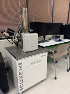
The Bruker eFlashXS detector is the ED-XS system that can be mounted on compact SEMs such as the Coxem CX-300 and EM-40. The detector features a CMOS sensor and a native resolution of 720×540. This is the most affordable and compact EDS/EBSD system; it is small, light, and easy to operate. We have the eFlashXS installed on our tabletop COXEM EM-40 and compact CX-300 SEM as well. COXEM is the first company to install EBSD detectors on a tabletop SEMs.
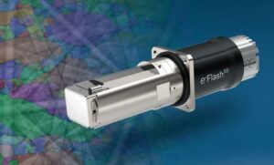
Bruker eFlash XS installed on Coxem EM-40
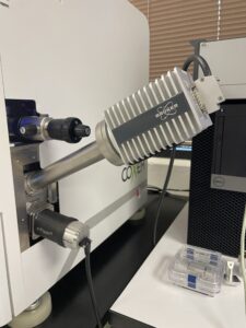
The other system is Bruker’s latest EBSD detector, eWARP, which uses a wide-area, pixelated detector. With direct electron detection technology, the eWARP detector enables high signal sensitivity, faster acquisition, and enables low-kV EBSD capability. The eWARP system is installed in our CIQTEK 5000X FE SEM, a high-resolution FE SEM with a large chamber.
Bruker eWARP installed on CIQTEK SEM5000X FE SEM
Objective
The objective of this study is to compare the performance of the eFlash XS and eWARP EBSD systems, highlighting their similarities and differences in crystallographic analysis.
Results and Discussion
Figure 2 shows an SEM image of the duplex steel after polishing. The BSE image clearly shows the grains with different contrast.
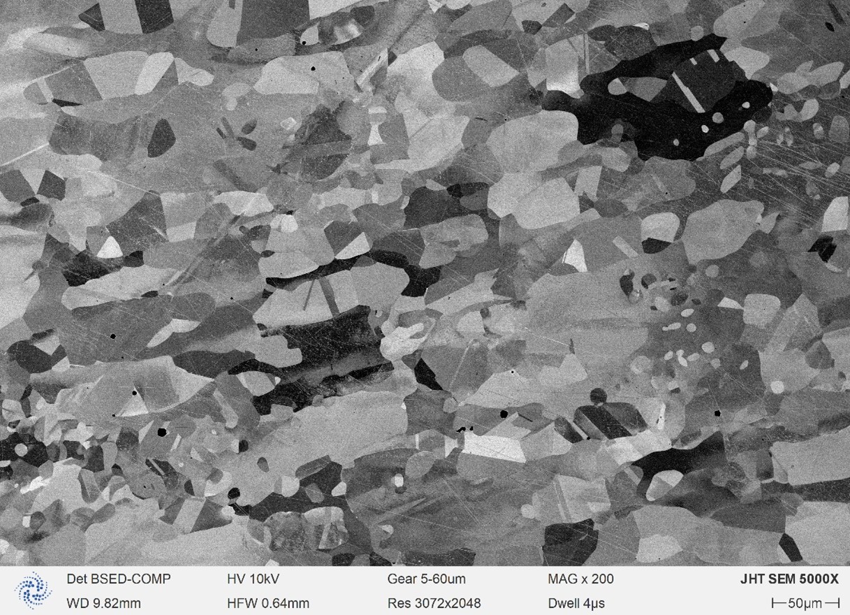 Figure 2: BSE image of the duplex steel surface after sample preparation.
To get a more direct comparison between the two EBSD systems, we use similar imaging conditions at 20kV on the SEM and a similar EBSD step size to get the grain information.
The comparison of the two EBSD acquisitions is shown in Table 1. Good sample preparation ensures that the indexing rate on the duplex steel between the two systems is high and identical. With a similar EBSD step size and the same map size, acquisition on eWARP is more than 40 times faster than eFlash XS EBSD, given its sensitive detector.
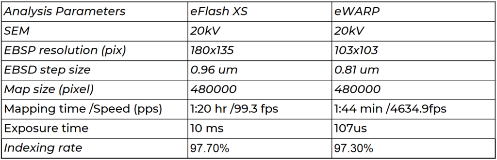 Table 1: EBSD mapping acquisition comparison between eFlash XS and eWARP EBSD detector
Figure 3 shows the results obtained using the eFlash XS EBSD detector, including (a) EBSD pattern, (b) pattern quality with phase map, (c) phase analysis, (d) grain map, and (e) grain distribution analysis. This compact eFlash XS EBSD detector is capable of generating full analysis on materials despite a slightly longer acquisition time.
(a)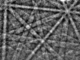 (b)
(b)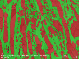
(c)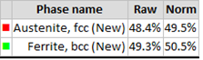
(d)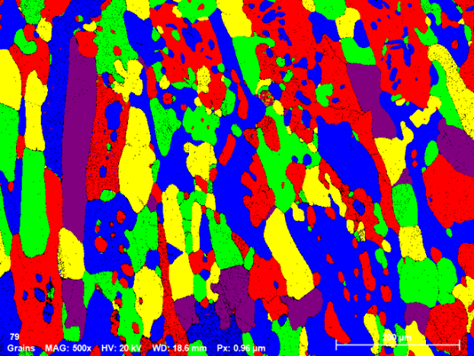
(e)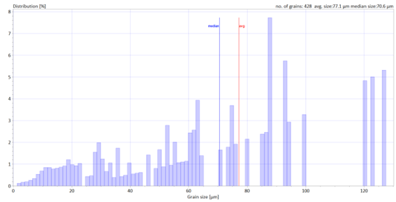 Figure 3: EBSD analysis on duplex steel using eFlash XS detector. Acquisition was performed on COXEM CX-300 compact tungsten SEM. (a) EBSD pattern, (b) pattern quality with phase map, (c) phase analysis, (d) grain map (e) grain distribution analysis
Experimental Procedure
A commercial duplex steel sample was prepared using Buehler sample preparation equipment, including:
- IsoMet High Speed Pro precision sectioning saw
- SimpliMet 4000 hot mounting system
- EcoMet 30 semi-automatic grinder-polisher
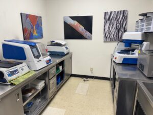
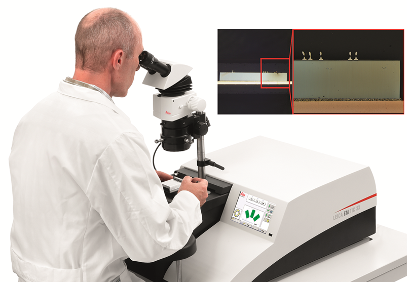
After polishing to a 0.05 μm finish, the sample was ion-milled at 3.5 kV using a Leica ion mill to remove residual surface stress. Ion milling is a critical step that significantly improves EBSD data quality and indexing accuracy:
- Leica EM TIC3X ion mill
The sample was analyzed using:
- A COXEM CX-300 tungsten SEM with an eFlash XS EBSD detector
- A CIQTEK 5000X FE-SEM with an eWARP EBSD detector
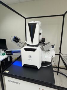
Figure 4 shows the results obtained using the eWARP EBSD detector, including (a) EBSD pattern, (b) pattern quality with phase map, (c) phase analysis, (d) grain map, and (e) grain distribution analysis, and (f) VFSE image.
With this sensitive EBSD detector, all statistical analyses can be performed with great precision within 1:44min, enabling fast routine EBSD analysis. The VFSE image is generated simultaneously with EBSD acquisition, revealing details of the grain structure.
(a)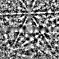 (b)
(b)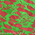
(c)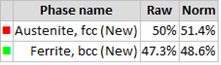
(d)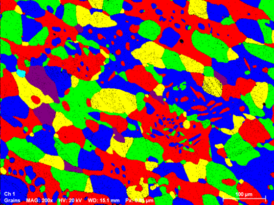
(e)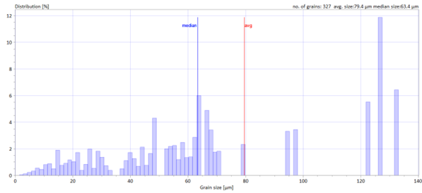
(f)
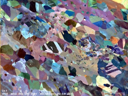
Figure 4: EBSD analysis on duplex steel using eWARP detector. Acquisition was performed on CIQTEK 5000X FE SEM. (a) EBSD pattern, (b) pattern quality with phase map, (c) phase analysis, (d) grain map (e) grain distribution analysis (f) VFSE image
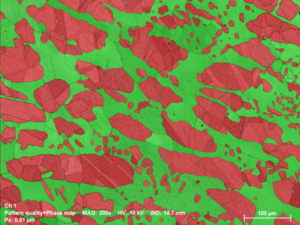
Another great advantage of the eWARP EBSD detector is its capability to perform analysis at low energy. Figure 5 shows the EBSD analysis on the duplex steel using eWARP at 10kV (a) pattern, (b) pattern quality with phase map. The EBSD analysis of the same map size can be completed within 2:12 min, with 93.9% indexing rate. Low-energy EBSD provides better spatial resolution for grain analysis due to the smaller interaction volume. This is beneficial for small-grain analysis and reduces beam damage on sensitive materials.
(a)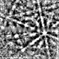 (b)
(b)